

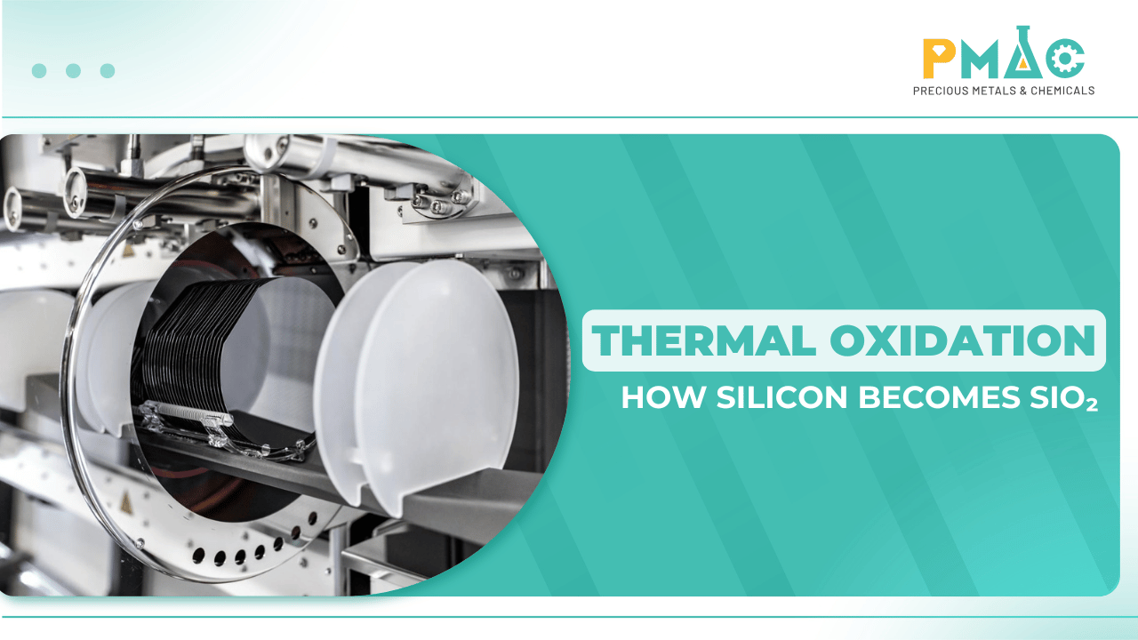
Not every material layer in a semiconductor chip is deposited onto a wafer from an external source. Some layers are formed through chemical reactions with the silicon substrate itself. One important example is silicon dioxide (SiO₂), which can be grown directly on a silicon wafer through thermal oxidation.
Although SiO₂ does not conduct electricity, it plays an essential role in electrical insulation, surface protection, and the formation of semiconductor structures. Producing a suitable oxide layer, however, involves more than creating the right material. Its thickness, uniformity, electrical properties, and interface quality must all meet the requirements of the intended fabrication process.
I. What Is Silicon Thermal Oxidation?
Silicon thermal oxidation is a high-temperature process in which silicon reacts with oxygen or water vapor to form a silicon dioxide (SiO₂) layer directly on the wafer surface.
Unlike thin-film deposition, which introduces material from an external source, thermal oxidation converts part of the existing silicon substrate into silicon dioxide. The resulting oxide is formed at the silicon surface, creating an interface between the newly grown SiO₂ layer and the underlying silicon.
The process is typically carried out in a controlled high-temperature furnace, where temperature, gas composition, and processing time are carefully regulated. Conventional silicon thermal oxidation commonly operates at temperatures of approximately 800–1,200°C, depending on the process conditions and desired oxide characteristics.
Two fundamental reactions describe the process:
- Dry oxidation: Si + O₂ → SiO₂
- Wet oxidation: Si + 2H₂O → SiO₂ + 2H₂
The difference lies in the oxidizing species. Dry oxidation uses oxygen, while wet oxidation uses water vapor. This distinction affects oxide growth rate, material properties, and the applications for which each process is suitable.
As explained by the University of Texas at El Paso, thermally grown silicon dioxide offers favorable dielectric properties and a relatively low-defect interface with silicon. These characteristics have contributed significantly to the widespread adoption of silicon in microelectronics.
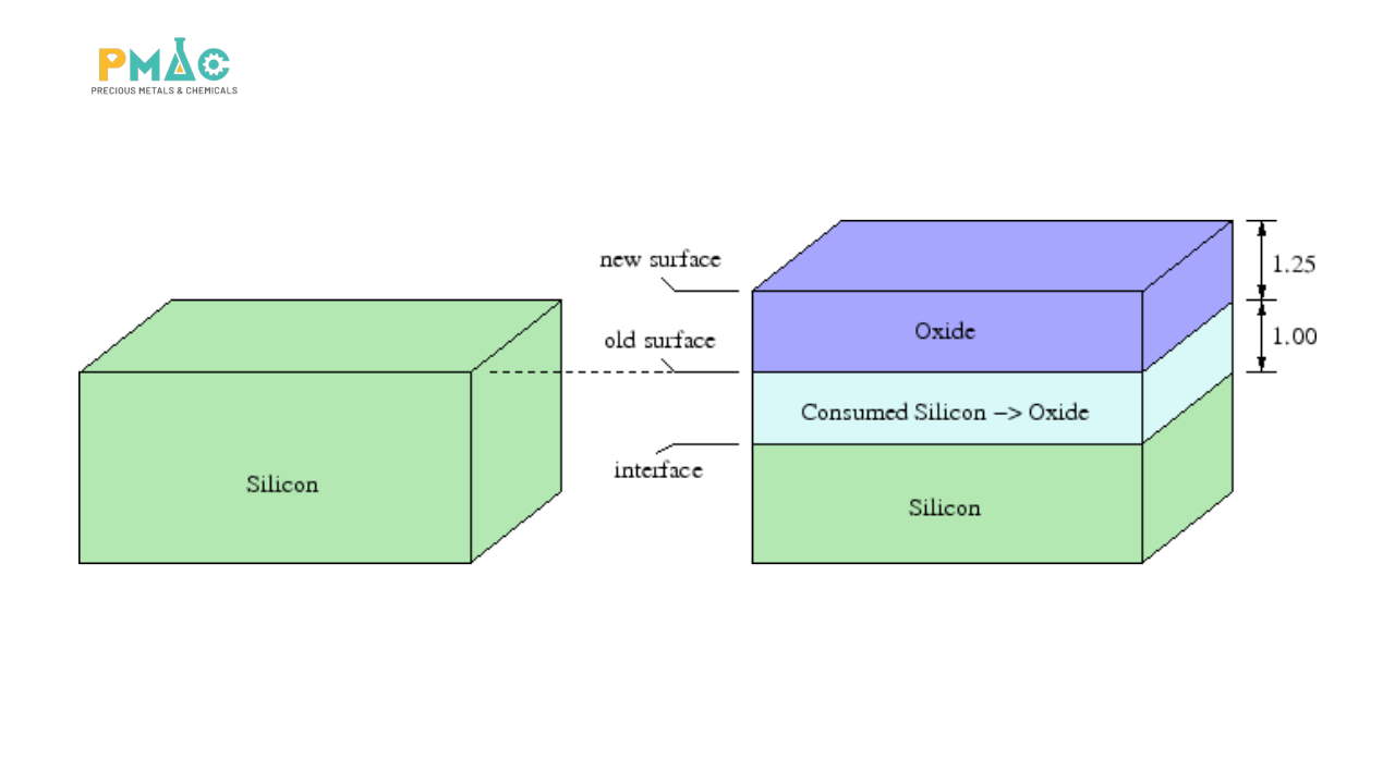
Figure 1. Diagram showing silicon consumption during thermal oxidation and SiO2 layer growth
II. Why Is Silicon Dioxide Important in Semiconductor Manufacturing?
Silicon serves as the foundation for many semiconductor devices, but the silicon substrate alone is not sufficient to build functional integrated circuits. Transistors and interconnect structures also require insulating materials, protective layers, and precisely defined regions for subsequent processing.
Silicon dioxide has been widely used for these purposes because of its insulating properties and its ability to form a well-controlled interface with silicon. Depending on the device architecture and fabrication process, SiO₂ can perform several different functions.
1. Electrical Insulation and Device Isolation
In an integrated circuit, conductive regions and neighboring devices must be electrically isolated to prevent unintended current paths. Silicon dioxide, with its high electrical resistivity and dielectric properties, has long been used in semiconductor isolation structures.
In earlier generations of CMOS manufacturing, field oxide layers were commonly formed using local oxidation of silicon (LOCOS). This process selectively grew relatively thick oxide regions to isolate active device areas.
As transistor density increased, LOCOS was progressively replaced in many technologies by shallow trench isolation (STI). In STI, narrow trenches are etched into the silicon and subsequently filled with a suitable dielectric material, often deposited silicon dioxide.
This transition illustrates an important distinction: SiO₂ remains valuable as an insulating material, but its placement and the methods used to form it have evolved with semiconductor technology.
2. Surface Protection and Passivation
Silicon surfaces can be affected by environmental exposure, unwanted impurities, and subsequent processing steps. In suitable applications, SiO₂ can serve as a protective or passivation layer, helping stabilize surface conditions and reduce undesirable interactions.
However, oxide formation does not automatically guarantee a high-quality surface. Contamination before oxidation, defects at the silicon–oxide interface, or unsuitable processing conditions can still affect electrical performance and device reliability.
Surface preparation therefore plays an important role in thermal oxidation. Wafers must be cleaned and contamination controlled before oxidation to reduce the risk of defects being incorporated into the growing oxide layer.
3. Masking During Semiconductor Processing
Silicon dioxide can also serve as a masking material during certain fabrication steps. Once an oxide layer has been patterned, selected regions may be protected while other areas undergo etching, diffusion, ion implantation, or additional processing.
The effectiveness of an oxide mask depends on factors such as oxide thickness, the process being performed, and the materials or chemicals involved. Not every SiO₂ layer is suitable for every masking application.
Patterning an oxide layer typically involves a combination of photolithography and selective etching. Photolithography defines the regions that need to be processed, while etching transfers the required pattern into the underlying material.
4. Gate Dielectrics in Transistor Structures
One of silicon dioxide’s most important historical applications is as the gate dielectric in metal-oxide-semiconductor (MOS) transistors.
The gate dielectric separates the gate electrode from the semiconductor channel, allowing an electric field to control current flow without direct conductive contact between the two regions.
For many generations of conventional CMOS technology, thermally grown SiO₂ was widely used because of its electrical insulation properties and high-quality interface with silicon.
However, continued transistor scaling introduced a major limitation. As SiO₂ gate dielectrics became extremely thin, quantum tunneling increased leakage current, creating challenges for power consumption and device performance.
To address this problem, many advanced logic technologies adopted high-k dielectric materials combined with metal gate electrodes. As Intel explains, higher dielectric constant materials can provide the required electrical characteristics with a greater physical thickness, helping reduce gate leakage.
Therefore, it would be inaccurate to assume that every modern transistor still uses pure SiO₂ as its primary gate dielectric. The role of silicon dioxide depends on the device structure, manufacturing generation, and specific application.
III. Dry Oxidation vs. Wet Oxidation: Which Process Is More Suitable?
Both dry and wet oxidation convert silicon into SiO₂, but they operate with different oxidizing environments. This affects how quickly the oxide grows, how its thickness can be controlled, and which properties are most suitable for the intended application.
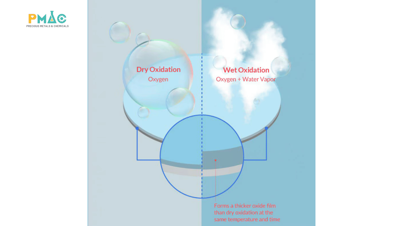
Figure 2. Comparison of dry oxidation and wet oxidation
1. Dry Oxidation: Greater Control for Thin Oxide Layers
During dry oxidation, silicon wafers are heated in an oxygen-containing environment. Oxygen passes through the oxide layer already formed and continues reacting with silicon at the silicon–SiO₂ interface, allowing the oxide to grow over time.
Dry oxidation generally produces slower oxide growth than wet oxidation under comparable conditions. However, it is particularly useful for producing relatively thin oxide layers with well-controlled thickness and favorable dielectric properties.
This is why dry oxidation was extensively used for high-quality gate oxides in conventional MOS technologies and remains relevant to processes requiring carefully controlled thermal oxide layers.
Its slower growth rate can also be a limitation. Producing a relatively thick oxide may require longer processing times, potentially affecting furnace throughput and operating costs.
2. Wet Oxidation: Faster Growth for Thicker Oxide Layers
Wet oxidation uses water vapor as the oxidizing species. Under comparable conditions, water vapor generally enables faster oxide growth than dry oxygen.
This makes wet oxidation useful when relatively thick silicon dioxide layers are required within a practical processing time. Applications may include certain insulating or protective oxide structures where the required material properties can be achieved using this approach.
However, faster oxide growth does not necessarily mean better performance. Where electrical characteristics and interface quality are particularly critical, dry oxidation may be the more appropriate option.
The choice must therefore reflect the function of the oxide rather than growth rate alone.
| Evaluation Criteria | Dry Oxidation | Wet Oxidation |
| Oxidizing species | Oxygen (O₂) | Water vapor (H₂O) |
| Oxide growth rate | Generally slower | Generally faster |
| Typical thickness preference | Relatively thin oxide layers | Relatively thick oxide layers |
| Dielectric properties | Often favorable for demanding electrical applications | Must be evaluated against application requirements |
| Common applications | Thin oxides, high-quality dielectric layers | Thicker insulating or protective oxides |
| Main consideration | Longer processing times for thick oxides | Oxide characteristics and interface quality |
Semiconductor manufacturers must also consider that actual growth rates depend on temperature, initial oxide thickness, silicon properties, and other process conditions.
As outlined by Samsung Semiconductor, dry oxidation is well suited to forming thinner oxides with strong electrical properties, while wet oxidation offers a higher growth rate for thicker layers.
IV. How Does the Thermal Oxidation Process Work?
In a conventional thermal oxidation process, silicon wafers are placed inside a high-temperature processing system capable of maintaining a controlled oxygen or steam environment. As the temperature rises, the oxidizing species reacts with silicon to form SiO₂.
Importantly, oxide growth does not occur simply by depositing additional material onto the outer surface. Once an initial oxide layer has formed, oxidizing species must move through that layer to reach the silicon–oxide interface, where further reactions occur.
As the oxide becomes thicker, the growing layer increasingly limits transport of the oxidizing species, so the growth rate generally decreases.
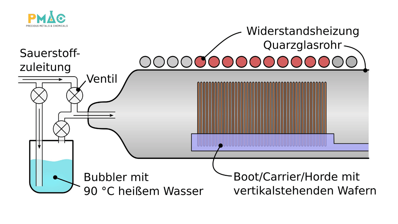
Figure 3. Diagram of a thermal oxidation furnace showing heating elements and silicon wafer placement
The process can be understood through four main stages.
1. Wafer Preparation and Surface Cleaning
Before oxidation, the wafer must meet the cleanliness and surface-quality requirements of the process. Residual particles, organic contamination, and metallic impurities can affect oxide growth and the quality of the silicon–oxide interface.
An appropriate cleaning process must therefore be selected based on the wafer material, existing surface layers, and oxidation requirements. Cleaning methods suitable for bare silicon may not be appropriate for wafers containing previously fabricated structures.
PMAC’s semiconductor portfolio includes wet-processing and wafer-cleaning equipment, together with high-purity process chemicals. These technology categories are relevant to surface preparation before high-temperature processing, where controlling contamination is particularly important.
2. Heating Under Controlled Conditions
After preparation, wafers are loaded into a furnace and processed according to a defined temperature and gas-flow program.
The system must maintain the required processing conditions, including temperature, oxidizing atmosphere, gas flow, and treatment duration. These variables influence oxide growth and the consistency of results across wafers.
Temperature stability becomes especially important when several wafers are processed in a single batch. Differences in local temperature or gas conditions can contribute to variations in oxide thickness.
For this reason, furnace performance should not be evaluated solely by its maximum operating temperature. Process stability, uniformity, and repeatability are equally important.
3. Silicon Dioxide Formation and Growth
As oxidation proceeds, silicon at the wafer surface reacts with oxygen or water vapor to produce silicon dioxide.
The oxide continues to grow as oxidizing species pass through the existing layer and reach the silicon underneath. This is the defining difference between thermal oxidation and conventional thin-film deposition. Thermal oxidation consumes part of the silicon substrate while creating a thicker oxide layer.
According to the Colorado School of Mines, the thickness of silicon consumed is approximately 44% of the final thickness of the thermally grown SiO₂ layer.
For example, forming a 100 nm thermal oxide on an initially bare silicon surface consumes approximately 44 nm of silicon. The oxide extends both into the original silicon surface and above it because silicon dioxide occupies a larger volume than the silicon consumed.
This relationship is a useful approximation for understanding material consumption and oxide geometry, rather than a guaranteed process result under every condition.
4. Cooling and Oxide Quality Verification
Once the specified processing conditions have been completed, wafers are cooled and transferred for appropriate inspection or measurement.
Important parameters may include oxide thickness, within-wafer uniformity, surface condition, and the material characteristics required by the next fabrication step.
For applications involving demanding dielectric requirements, additional electrical measurements may be necessary to evaluate leakage, breakdown behavior, interface defects, or reliability.
The process should therefore not be considered successful simply because the specified furnace temperature and treatment time were reached. The resulting SiO₂ layer must be verified against the application’s actual quality requirements.
V. What Determines the Quality of a Thermally Grown SiO₂ Layer?
Two wafers processed for the same duration may not necessarily develop oxide layers with identical thickness or properties.
Oxide growth depends on temperature, oxidizing atmosphere, silicon substrate characteristics, and initial surface conditions. These factors must be considered together when developing a process or evaluating equipment performance.
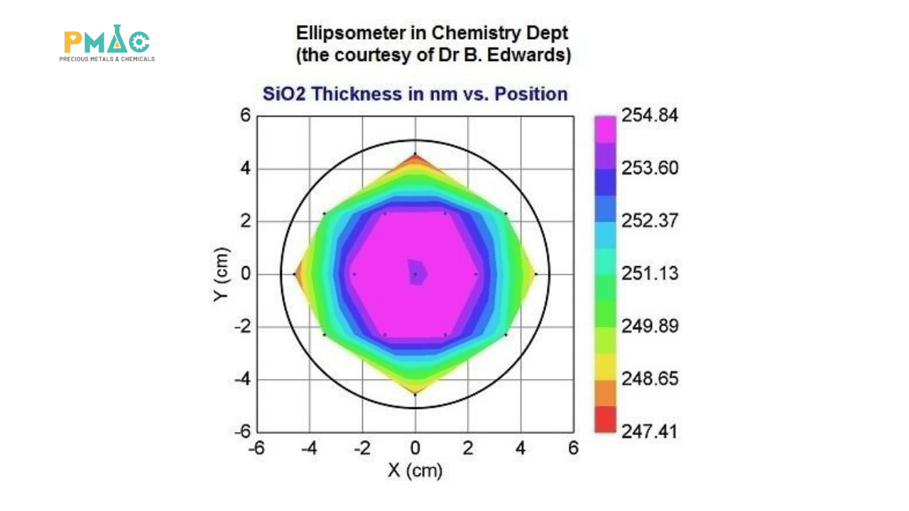
Figure 4. Ellipsometry thickness map showing SiO2 film thickness variation across a silicon wafer
1. Oxidation Temperature and Processing Time
Temperature directly influences reaction kinetics and the transport of oxidizing species through the growing oxide.
Higher temperatures generally increase oxide growth rates, but they also impose a greater thermal load on the wafer and any structures already present.
Processing time determines how long the reaction is allowed to continue. However, oxide growth is not necessarily linear with time, because an increasingly thick oxide layer can slow the movement of oxidizing species toward the silicon surface.
For this reason, oxidation time should be established using the target thickness, wafer characteristics, and growth behavior validated for the actual process conditions.
2. Oxidizing Atmosphere and Chemical Purity
The composition and purity of the oxidizing environment can influence oxide quality.
Unwanted contaminants introduced through process gases, steam, equipment surfaces, or handling systems may affect the silicon–oxide interface or other properties that need to be tightly controlled.
Manufacturers must therefore evaluate gas purity, delivery systems, furnace cleanliness, and process conditions according to the application’s requirements.
Maintaining suitable material quality is particularly important when producing oxide layers for electrically sensitive structures.
3. Silicon Substrate Properties and Surface Condition
Oxidation behavior can vary with silicon crystal orientation, doping concentration, and the initial condition of the surface.
These differences should be considered when transferring a process between wafer types or evaluating repeatability across production lots.
Residual contamination or native oxides may also influence the starting conditions. Consequently, incoming wafer specifications and cleaning performance form part of the broader oxidation quality-control strategy.
4. Oxide Thickness and Uniformity
An SiO₂ layer may achieve the required average thickness while still exhibiting unacceptable variations across the wafer. For sensitive applications, these variations can affect electrical characteristics or the performance of subsequent processing steps.
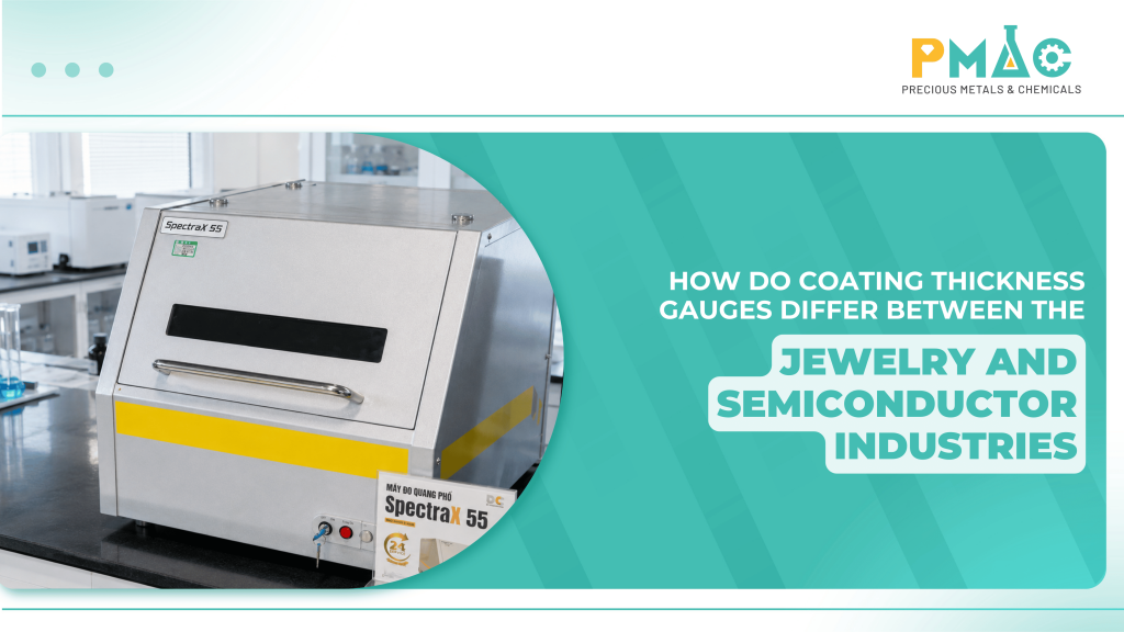
Optical measurement methods such as ellipsometry or reflectometry may be used to evaluate oxide thickness and uniformity when appropriate for the sample structure and measurement range.
PMAC’s semiconductor metrology portfolio includes thin-film thickness measurement and ellipsometry-related technologies. Selecting a suitable method requires consideration of the oxide material, layer structure, measurement range, and required accuracy.
VI. Thermal Oxidation vs. SiO₂ Deposition: What Is the Difference?
Silicon dioxide does not have to be produced through thermal oxidation. It can also be formed using thin-film deposition technologies such as chemical vapor deposition (CVD), including process variants designed for different materials and thermal requirements.
The fundamental difference is how the material layer is created.
In thermal oxidation, the silicon substrate itself reacts with an oxidizing species to form SiO₂. In CVD, externally supplied chemical precursors react to produce a film on the wafer surface.
These different mechanisms influence substrate compatibility, processing temperature, interface characteristics, and the opportunities for integration into the overall manufacturing flow.
| Criteria | Silicon Thermal Oxidation | SiO₂ Deposition by CVD |
| Film formation | Converts part of the silicon substrate into SiO₂ | Forms SiO₂ using externally supplied chemical precursors |
| Substrate requirements | Requires accessible silicon capable of undergoing oxidation | Can deposit films on a wider range of suitable surfaces |
| Silicon consumption | Yes | Not through the same substrate-oxidation mechanism |
| Processing temperature | Typically high | Depends on the CVD method; lower-temperature options are available |
| Silicon–oxide interface | Often offers excellent interface properties under suitable conditions | Depends on the deposition process and subsequent treatments |
| Typical applications | Directly grown silicon oxides, selected insulating and protective layers | Dielectric films and insulating layers on various semiconductor structures |
Thermal oxidation offers important advantages when a high-quality silicon–SiO₂ interface is required. However, its high processing temperature may limit its use on wafers containing materials or structures that cannot tolerate substantial thermal exposure.
CVD provides greater flexibility in terms of substrate materials and deposition conditions. Its performance, however, depends on process chemistry, precursor selection, equipment configuration, and the requirements of the resulting film.
Neither method is universally superior. The correct choice depends on the intended function of the SiO₂ layer, wafer condition, allowable thermal budget, and overall process requirements.
For a broader comparison of thin-film formation technologies, explore PMAC’s article: How Are PVD, CVD, and ALD Different?.
VII. Thermal Oxidation Within PMAC’s Semiconductor Technology Portfolio
In semiconductor fabrication, oxide quality depends on more than the high-temperature treatment itself. Wafer preparation, process materials, equipment conditions, and post-process measurement all contribute to the final result.
For manufacturers evaluating thermal processing technologies, the relevant questions extend beyond furnace temperature and processing time. They also include the cleanliness of the incoming wafer, control of the oxidizing environment, process uniformity, and the ability to verify the resulting oxide layer.
PMAC’s semiconductor portfolio includes wafer-cleaning and wet-processing equipment, high-purity process chemicals, thermal-processing equipment categories, and analytical and metrology technologies.
These capabilities can support the evaluation of different needs across wafer preparation, high-temperature processing, and thin-film quality control.
For thermal oxidation specifically, the equipment configuration must be assessed against the required oxidizing atmosphere, temperature control, processing time, wafer compatibility, and uniformity requirements.
Not every annealing furnace is automatically suitable for controlled silicon thermal oxidation. A system’s capabilities must be verified for the intended process rather than inferred from its temperature range alone.
Beyond equipment and materials, PMAC aims to support manufacturers through technical consultation, solution evaluation, installation, commissioning, training, and maintenance.
This integrated approach allows individual process requirements to be considered within the context of the broader manufacturing line, helping companies evaluate appropriate technologies rather than selecting isolated equipment based solely on published specifications.
VIII. Frequently Asked Questions About Silicon Thermal Oxidation
1. Is Thermal Oxidation the Same as Depositing SiO₂ on a Wafer?
No. Thermal oxidation forms silicon dioxide through a chemical reaction between the silicon substrate and an oxidizing species at elevated temperature. Part of the silicon is consumed as the oxide grows.
In contrast, deposition methods such as CVD use externally supplied reactants to form a film on the wafer surface. Because their formation mechanisms differ, the methods have different material requirements, process characteristics, and applications.
2. Why Does Silicon Thermal Oxidation Require High Temperatures?
Elevated temperatures promote the chemical reaction between silicon and the oxidizing species while supporting transport through the growing oxide layer.
The appropriate temperature depends on the desired oxide thickness, wafer type, process equipment, and quality requirements. Manufacturers must balance growth rate against the thermal effects on the substrate and any existing structures.
3. Is Dry Oxidation Better Than Wet Oxidation?
Neither method is universally better.
Dry oxidation is often preferred for relatively thin oxides requiring favorable dielectric properties and interface quality. Wet oxidation provides faster growth and can be more practical for thicker oxide layers.
The choice depends on the intended application, equipment capabilities, processing time, and required oxide characteristics.
4. Is Silicon Dioxide Still Used in Modern Semiconductor Chips?
Yes. Silicon dioxide continues to serve important functions in various insulating, protective, and dielectric structures.
However, its applications and formation methods have evolved. Many advanced logic technologies now use high-k materials instead of pure SiO₂ as the primary gate dielectric, while silicon dioxide remains relevant in other parts of semiconductor fabrication.
5. How Can Manufacturers Verify the Quality of a Thermally Grown SiO₂ Layer?
Oxide quality must be evaluated against the layer’s intended function and technical specifications.
Common considerations include thickness, uniformity, surface condition, and material properties. For demanding dielectric applications, additional electrical or reliability measurements may be needed.
Furnace temperature and treatment time alone are not sufficient to confirm that the final oxide meets process requirements.
Conclusion
Silicon thermal oxidation is an important semiconductor manufacturing process that forms SiO₂ directly from the silicon wafer surface. Depending on the device architecture and fabrication stage, the resulting oxide can provide electrical insulation, surface protection, or masking functionality.
However, successfully growing an oxide layer does not automatically mean the process meets its specifications. Oxide performance depends on the oxidation method, thermal conditions, surface cleanliness, substrate properties, and subsequent quality verification.
Contact PMAC to discuss your wafer materials, process requirements, and technical evaluation criteria. Our team can help you explore relevant technology categories within PMAC’s semiconductor portfolio and identify suitable options for your application.
PMAC Joint Stock Company
Ho Chi Minh City Office:
4th Floor, HUTECH Building, D1 Road, Saigon Hi-Tech Park, Tang Nhon Phu Ward, Ho Chi Minh City, Vietnam
Hanoi Office:
22B O2, Linh Dam Peninsula, Hoang Liet Ward, Hanoi, Vietnam
Hotline: +84 387 235 878
Facebook: PMAC

Author: PMAC – Nguyen Quoc Dung – Lab & Maintenance Center Chief