

Over the past few years, GPUs have become almost synonymous with the artificial intelligence boom. The rise of large language models (LLMs), generative AI, and multimodal systems has driven a sharp increase in demand for computing power, leading to massive investment in GPUs and accelerators for data centers.
By 2026, the scale of this trend has become increasingly visible across the semiconductor industry. According to Deloitte’s 2026 Semiconductor Industry Outlook, global semiconductor revenue could reach approximately USD 975 billion this year, with chips serving generative AI applications projected to account for nearly USD 500 billion. What stands out is that AI chips represent a very high share of market value while accounting for only a small fraction of total semiconductor unit shipments, showing how AI is reshaping where value is concentrated within the industry.
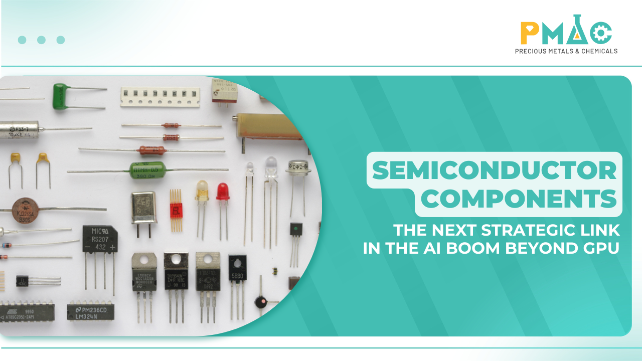
However, the GPU boom is only part of the story. When thousands of processors operate together in an AI cluster, system performance increasingly depends on how quickly data can be delivered to processors, how efficiently chips can communicate with one another, how power is supplied, and how multiple components are integrated into the same system. This shift is bringing many semiconductor components that once sat behind the GPU into strategic roles within AI infrastructure.
I. Graphics Processing Units (GPUs) and the AI Boom
1. GPUs in AI Infrastructure
GPUs were originally developed for graphics processing, but their ability to perform large numbers of parallel computations makes them particularly well suited to AI model training and inference. As model sizes increase, hundreds or even thousands of GPUs can be connected into clusters to process enormous volumes of data together.
This development has significantly changed the structure of the semiconductor market. According to Deloitte, AI is becoming the main driver pushing semiconductor industry revenue toward record levels in 2026, while many traditional segments such as smartphones, personal computers, and several non-data-center applications are growing more slowly.
GPUs therefore remain central to AI infrastructure. However, as GPU counts and computing capacity continue to rise, the rest of the system must scale at a similar pace. If data cannot reach the GPU quickly enough or processors cannot exchange data efficiently, much of the additional computing capacity may remain underutilized.
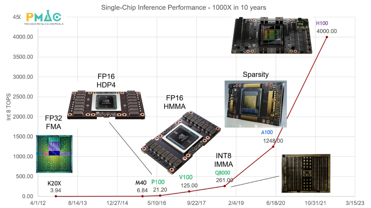
Figure 1. GPU performance has increased dramatically across generations, driving the development of AI infrastructure
2. System-Level AI Performance
A modern AI system can be viewed as the interaction of compute, memory, data connectivity, power delivery, and packaging. Each element has its own limitations, and a bottleneck in any one of them can affect overall system performance.
This trend has become particularly visible in 2026. Deloitte also notes that competition is increasingly moving toward system-level performance, where processors, HBM, chiplets, and network infrastructure need to be integrated more closely. Meanwhile, a Gartner analysis published in May 2026 suggests that key AI infrastructure bottlenecks in 2026–2027 are increasingly concentrated around HBM and advanced packaging, rather than the accelerator chip alone.
This perspective helps explain why the market for AI semiconductor components is expanding beyond GPUs. Value is shifting toward components that allow GPUs to receive data faster, communicate with more processors, and operate more efficiently within increasingly dense computing clusters.
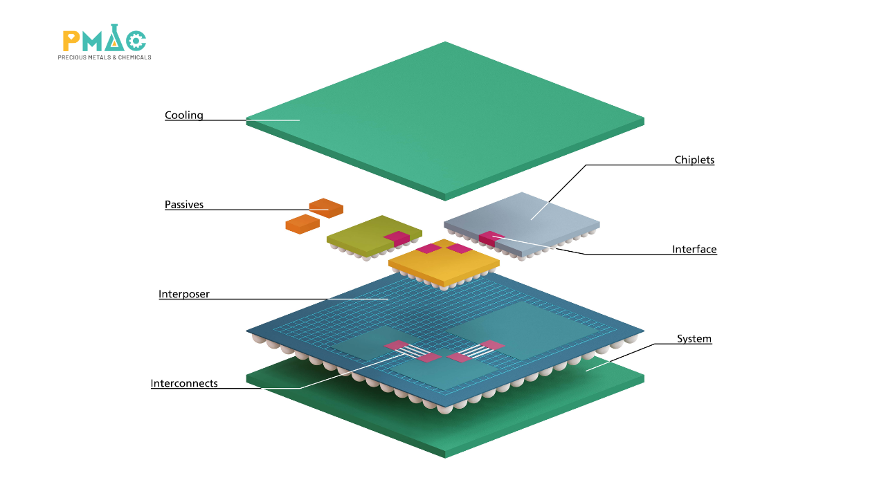
Figure 2. A modern chip system integrates multiple components through advanced packaging technologies
II. The Shift in the Semiconductor Components Market
1. Memory
GPUs can perform enormous amounts of computation, but those calculations require a continuous supply of data. If memory bandwidth cannot keep pace, the processor must wait for data, preventing available computing capacity from being fully utilized.
This is why HBM – High-Bandwidth Memory has become one of the most important components in modern AI chips. HBM stacks multiple DRAM layers and places them very close to the processor through advanced packaging technologies, significantly increasing data bandwidth while reducing the physical distance between memory and compute.
The importance of HBM now extends beyond technical performance and directly affects the AI chip market. In September 2026, Reuters reported that HBM shortages contributed to price increases among several Chinese AI accelerator manufacturers, demonstrating how memory supply can become a real bottleneck for the entire system.
PMAC has discussed stacked DRAM structures, TSV technology, and the role of high-bandwidth memory in greater detail in the article What Is HBM? Why Do AI Chips Need High-Bandwidth Memory?.
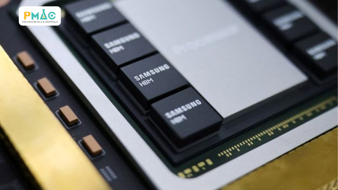
Figure 3. HBM is positioned close to the processor to meet the growing bandwidth requirements of AI
2. Data Connectivity and the Rise of Optical Interconnects
When an AI cluster contains thousands of GPUs, the amount of data moving between processors increases dramatically. In this environment, the speed of each individual GPU is only one part of the equation; the entire network connecting GPUs, memory, servers, and compute clusters must provide comparable bandwidth.
Deloitte forecasts that spending on AI networking will continue to grow rapidly in the coming years, while traditional copper-based electrical interconnects face increasing challenges in bandwidth, power consumption, and transmission distance as AI clusters scale. This is one of the forces pushing optical connectivity deeper into data-center architectures.
The trend is particularly visible in CPO – Co-Packaged Optics, where optical components are moved closer to networking chips to shorten electrical transmission paths. According to TrendForce, the CPO and NPO market is projected to grow from approximately USD 100 million in 2025 to more than USD 39 billion by 2030 as AI data centers shift toward higher-density optical connectivity.
3. Power Requirements
More powerful GPU clusters require more electricity and generate more heat. Power infrastructure is therefore becoming an increasingly important part of AI architecture rather than simply supporting infrastructure behind the server.
Power semiconductor components based on silicon carbide (SiC) and gallium nitride (GaN) are attracting increasing attention because of their ability to operate efficiently at high voltages or switching frequencies in suitable applications. TrendForce notes that SiC and GaN are entering a broader deployment phase in 2026, with demand from AI data centers emerging as one of the key drivers as power requirements approach new limits.
Read more: How Are Silicon, SiC, and GaN Different? Why Is Each Material Suited to Different Applications?
Deloitte also projects that the market for power supplies used in AI servers could grow from approximately USD 1.5 billion in 2024 to more than USD 31 billion by 2028. As power density per rack continues to rise, power architecture, voltage conversion, and power semiconductor efficiency will increasingly influence the scalability of data centers.
4. Packaging Technology
Another major change is taking place in the way semiconductor components are positioned relative to one another. Instead of leaving processors, memory, and other components farther apart on a circuit board, advanced packaging technologies bring them closer together to shorten data paths and increase interconnection density.
This is particularly important for AI because GPUs and accelerators must continuously exchange data with multiple HBM stacks. Technologies such as interposers, 2.5D/3D integration, and high-density interconnects are therefore becoming direct elements of the system architecture.
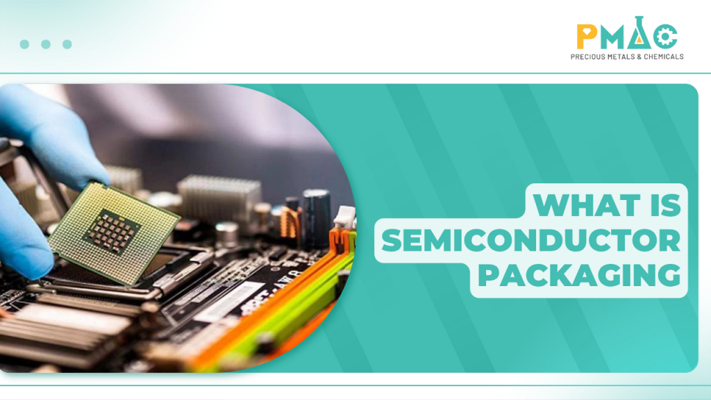
PMAC has discussed this transition in What Is Semiconductor Packaging? Why Do Semiconductor Chips Need Packaging?, where the role of packaging is evolving from basic chip protection toward supporting connectivity, power delivery, thermal management, and the integration of multiple components within the same system.
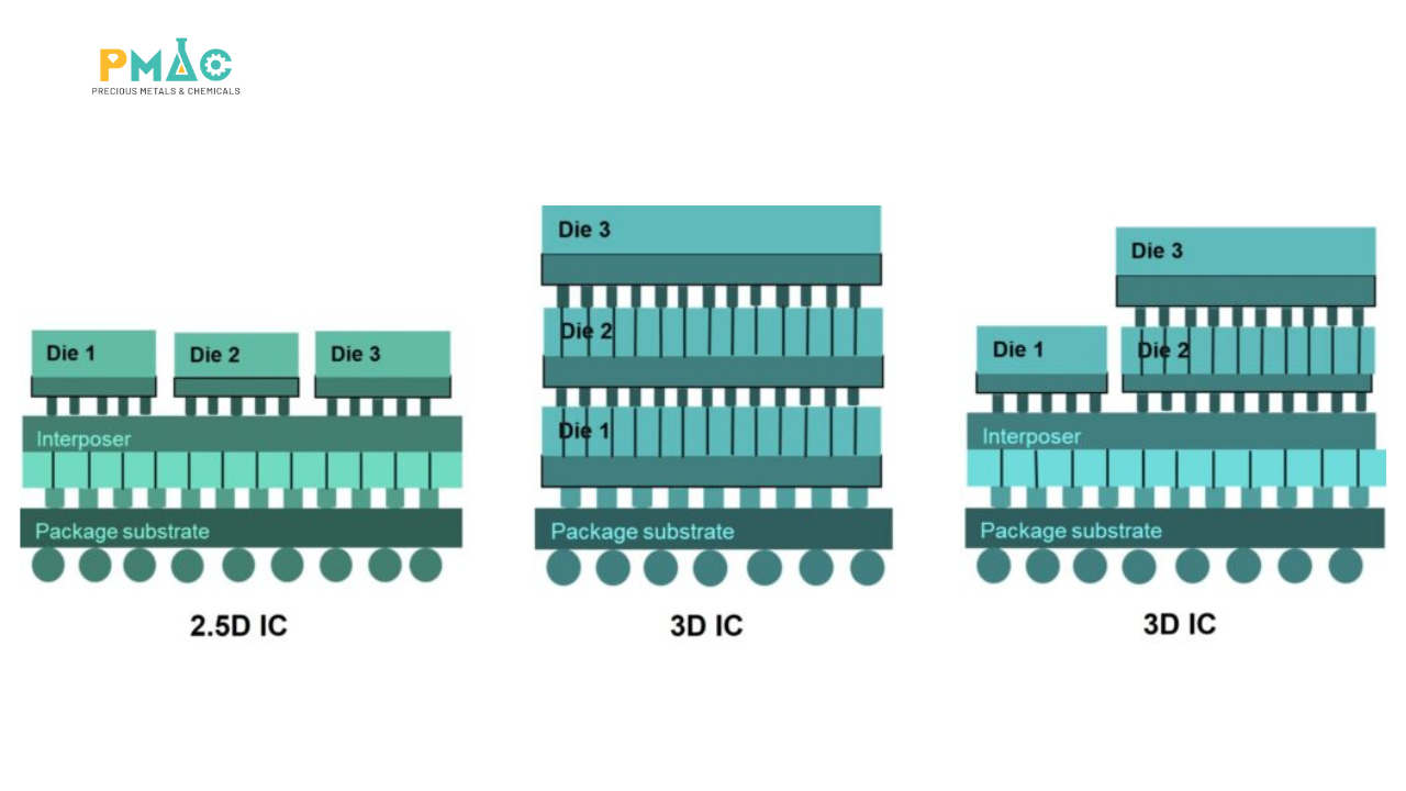
Figure 4. 2.5D and 3D packaging architectures bring multiple dies closer together
III. Semiconductor Components Emerging Alongside the AI Boom
1. HBM4
HBM is currently one of the semiconductor component categories most directly connected to the AI boom. As model sizes and data volumes increase, memory bandwidth between processors and memory must continue to expand, driving the industry from HBM3E toward the next generation, HBM4.
In early 2026, TrendForce reported that Samsung, SK hynix, and Micron were entering the final stages of HBM4 qualification for next-generation AI platforms. This transition shows that memory is becoming increasingly integrated into accelerator architecture rather than being treated as a relatively independent component.
HBM4 also creates new requirements for packaging and connectivity because signal counts continue to rise while the physical distance between memory and logic must be reduced further. The development of HBM is therefore closely linked to chiplets, interposers, package substrates, and high-density interconnect technologies.
2. Specialized AI Accelerators
GPUs remain the dominant platform for AI, but the rapid expansion of inference is creating more room for ASICs and specialized AI accelerators. These chips can be optimized for specific models or workloads, allowing system designers to balance performance, power consumption, and cost more effectively.
This trend is becoming increasingly visible as cloud providers develop their own chips and semiconductor companies focus more heavily on inference accelerators. In September 2026, Reuters reported that d-Matrix was developing its Raptor processor for AI inference and integrating it with Nvidia’s NVLink Fusion interconnect technology, reflecting a model in which multiple types of accelerators can coexist within the same AI architecture.
The growth of ASICs, GPUs, and specialized accelerators is also increasing demand for heterogeneous integration, where individually optimized functional blocks can be combined rather than building the entire system on one very large monolithic die.
3. Networking Chips and Optical Components
Data transmission is becoming a new layer of value within the AI semiconductor market. High-speed switch chips, signal processors, optical control circuits, and silicon photonics components all contribute to moving data between thousands of processors inside data centers.
A notable signal appeared in September 2026 when STMicroelectronics stated that approximately 80% of its more than USD 2 billion AI data-center revenue target for 2027 was expected to come from chips supporting optical data links. This suggests that optical connectivity is developing into a significant semiconductor market alongside AI processors themselves.
A review published in Nature Electronics in August 2026 also highlighted how the enormous data volumes associated with AI and high-performance computing are exposing limitations in electrical interconnects related to loss, bandwidth, and energy consumption. CPO architectures and chip-to-chip optical links are seen as promising development directions, although the industry still needs to address challenges involving heat, manufacturability, and standardization.
4. SiC and GaN Power Semiconductors
SiC and GaN are often associated with electric vehicles and power electronics, but the growth of AI is creating another important application area. New data centers must convert and distribute significantly more power than before while minimizing losses at each conversion stage.
In suitable applications, SiC provides advantages at high voltage and power levels, while GaN can perform particularly well in high-frequency switching systems. As data centers move toward higher-voltage power architectures and greater rack density, both semiconductor material platforms are gaining additional opportunities.
The overall shift can be summarized as follows:
| Component / Technology | Role in AI Systems | Demand Driver |
| HBM/HBM4 | Provides high-speed data to GPUs and accelerators | Larger models and increasing memory-bandwidth requirements |
| ASICs / AI accelerators | Optimized computing for specific workloads | Growth of AI inference and demand for energy efficiency |
| Networking chips and optical components | Connect GPUs, servers, and AI clusters | Larger clusters and limitations of electrical interconnects |
| SiC/GaN | Power conversion and power management | Rising AI data-center power density |
| Chiplets | Integrate multiple functional blocks into one system | Rising cost and complexity of monolithic dies |
| HBM, interposers, and advanced packaging | Bring memory and logic closer together | Higher bandwidth, interconnect density, and performance requirements |
IV. Chiplets and Advanced Packaging
1. Chiplet Architecture
The development of AI is also driving a major architectural shift. Rather than integrating every function onto an increasingly large monolithic die, designers can divide the system into multiple chiplets with dedicated functions and connect them through advanced packaging technologies.
This approach allows logic, memory, and interface blocks to use manufacturing processes better suited to their specific functions. It also enables greater design reuse and can reduce some of the yield-related risks associated with increasingly large dies.
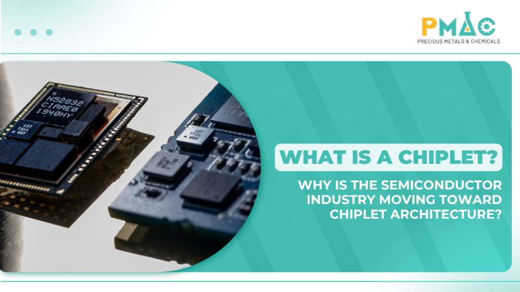
PMAC has discussed this architecture in greater detail in What Is a Chiplet? Why Is the Semiconductor Industry Moving Toward Chiplet Architectures?. When chiplets are combined with HBM, packaging becomes even more important because the package must simultaneously manage interconnect density, data transmission, power delivery, and thermal performance.
2. Package Substrates
As the number of chiplets and HBM stacks increases, package dimensions become larger while interconnect pitches continue to shrink. This places increasing pressure on substrate flatness, dimensional stability, and thermal properties.
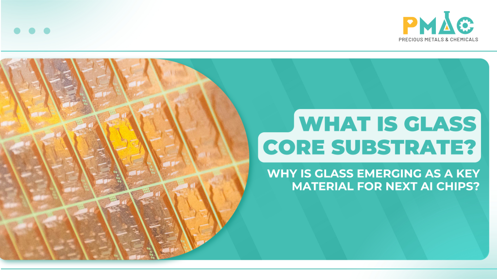
This is one reason glass is being investigated for future generations of package substrates. PMAC has explored this topic in What Is a Glass Core Substrate? Why Is Glass Being Considered for Next-Generation AI Chips?, where the dimensional stability of glass is discussed in the context of increasingly large AI packages and denser interconnection networks.
These changes at the wafer and package level show how the AI boom is reaching deeper into material layers that end users rarely see. As performance limitations shift from individual transistors toward system integration, substrates, interposers, and interconnect materials are beginning to directly influence the scalability of AI chips.
3. Thin-Film Deposition Technologies
Next-generation semiconductor components also place higher demands on the ultrathin material layers created during manufacturing. Metal films, diffusion barriers, dielectric layers, and other functional films must be tightly controlled in terms of thickness, composition, and uniformity.
PVD, CVD, and ALD address different requirements within this process. PVD has strong advantages for many metallic films, CVD provides broad material flexibility and high throughput, while ALD is particularly suitable for ultrathin films or three-dimensional structures requiring highly uniform coverage.
Read more: How Are PVD, CVD, and ALD Different?
For certain back-end wafer and packaging processes, surface treatment and electroplating also play important roles. Au, Pd, Ni, and Cu layers can influence conductivity, bonding, and component reliability. PMAC has discussed the connection between materials and manufacturing processes in Semiconductor Plating Materials: New Opportunities for PMAC and Umicore.
V. The Semiconductor Components Supply Chain
1. Materials
The expansion of AI is increasing demand for a wide range of materials behind finished semiconductor components, from Si, SiC, and GaN wafers to PVD targets, CVD/ALD precursors, high-purity chemicals, electroplating materials, bonding materials, and packaging consumables.
These materials directly affect process control. As semiconductor structures shrink and the number of material layers increases, acceptable contamination levels become lower, while lot-to-lot material consistency becomes increasingly important for manufacturing yield.
This expands the AI semiconductor market far beyond GPU designers. An AI system ultimately depends on a multi-layered supply network of material suppliers, equipment manufacturers, analytical technologies, packaging providers, and testing capabilities.
2. Equipment and Metrology
Increasingly complex semiconductor components require manufacturing and metrology equipment to evolve accordingly. PVD, CVD, ALD, plasma, etching, cleaning, and electroplating systems create the required material structures, while technologies such as XRF, ICP, SEM, X-ray systems, and thickness or profile measurement systems help verify whether processes remain within technical limits.
The importance of metrology increases as allowable process variation continues to shrink. Even a very small film, interconnect, or surface feature must maintain consistent properties across thousands of wafers and millions of components. Semiconductor manufacturing capability is therefore closely tied to the ability to measure, control, and trace quality data.
3. PMAC Ecosystem
This is also the direction PMAC is developing within the semiconductor sector. Building on its experience in materials, chemicals, surface treatment, analytical technologies, and laboratory solutions, PMAC is expanding its portfolio toward an integrated approach connecting semiconductor materials, process chemicals, manufacturing equipment, analytical and metrology solutions, packaging, and technical support.
Within this ecosystem, PMAC is developing solution groups ranging from Si, SiC, GaN, PVD materials, CVD/ALD precursors, and high-purity chemicals to wafer-processing equipment, electroplating solutions, analytical technologies, and process control.
Read more: PMAC Enters a New Phase: Building an Industrial Value-Creation Ecosystem
This approach aligns with the current transformation of the AI market. As performance increasingly shifts to the system level, manufacturers are moving beyond individual components toward the ability to connect materials – equipment – processes – metrology into a stable technology chain.
VI. Conclusion
The GPU boom is still continuing, but the development of AI in 2026 shows that value within the semiconductor market is spreading across a much broader system. HBM is becoming one of the clearest bottlenecks today; networking chips and optical components are gaining importance as AI clusters scale; SiC and GaN are being driven by power constraints; and chiplets together with advanced packaging are becoming essential platforms for integrating these components at higher density.
The next focal point of AI is therefore unlikely to be a single semiconductor component. The broader direction is a shift from competing solely on the power of an individual processor toward optimizing the entire system, where compute, memory, connectivity, power, and packaging must advance together.
This transition is also expanding opportunities throughout the semiconductor supply chain. The value created by AI is moving deeper into the materials, equipment, and technologies behind the chip, creating more opportunities for companies to participate in specialized parts of the value chain without having to begin by designing or manufacturing a complete GPU.
PMAC Joint Stock Company
Ho Chi Minh City Office:
4th Floor, HUTECH Building, D1 Road, Saigon Hi-Tech Park, Tang Nhon Phu Ward, Ho Chi Minh City, Vietnam
Hanoi Office:
22B O2, Linh Dam Peninsula, Hoang Liet Ward, Hanoi, Vietnam
Hotline: +84 387 235 878
Facebook: PMAC