

For many years, the semiconductor race largely focused on shrinking transistors to increase computing density on each chip. However, the rapid development of AI is shifting the performance bottleneck toward a different challenge: how to connect an increasing number of processors, chiplets, and HBM within the same system while maintaining high data-transfer speeds, structural stability, and manufacturability at scale.
As more components are integrated, the package must not only become larger but also maintain flatness, dimensional stability, and the precision required for an increasingly dense interconnect network. This tension between larger package sizes and tighter allowable tolerances is placing growing pressure on conventional package substrate materials.
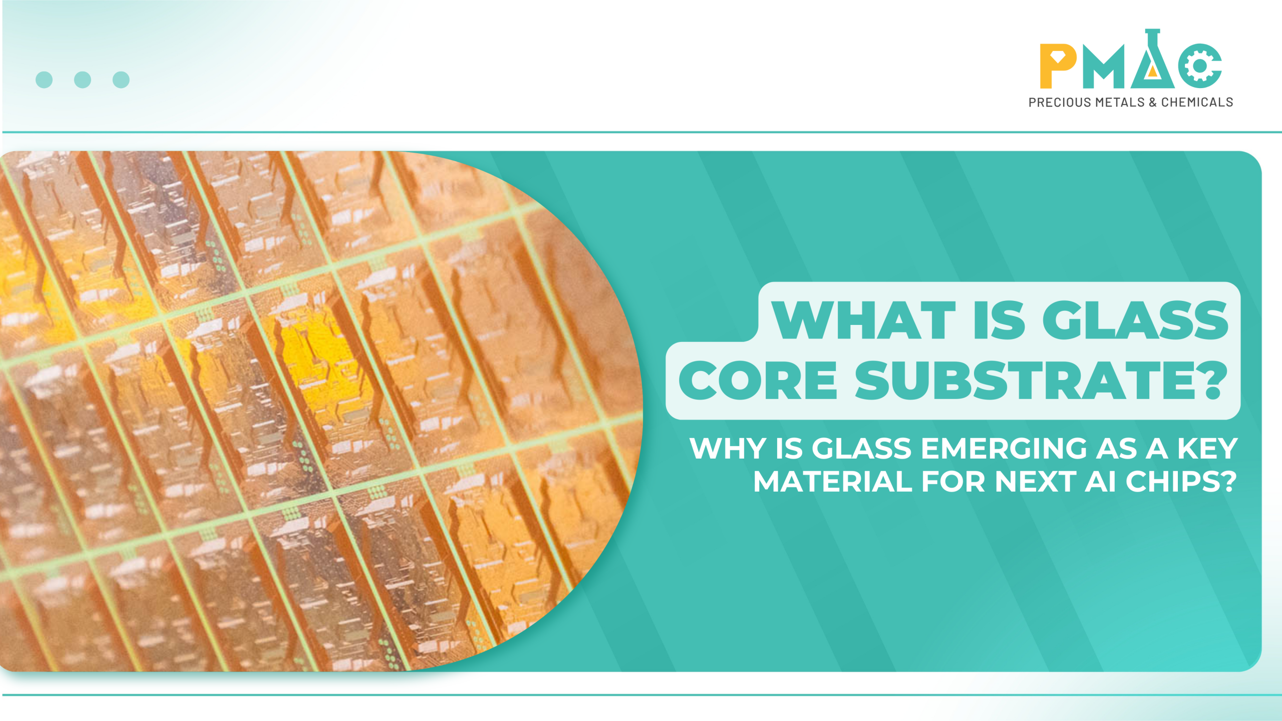
Against this backdrop, Glass Core Substrate is emerging as a promising material platform for the next generation of semiconductor packaging. Intel has researched glass substrate technology for more than a decade and has identified AI, data centers, and high-performance graphics as some of the first applications that could benefit from its advantages.
Interest in the technology is not limited to a single manufacturer. A 2026 SEMI report on Glass Core Substrate identifies AI, high-performance computing, and advanced packaging as key market drivers, while highlighting the advantages of glass in thermal stability, flatness, stiffness, electrical properties, and the ability to tailor the coefficient of thermal expansion to better match silicon.
To understand why these characteristics matter, Glass Core must be considered within the overall package structure. PMAC has explored this foundation in the article What Is Semiconductor Packaging and Why Do Chips Need Packaging?.
I. What Is Glass Core Substrate?
Before examining Glass Core Substrate, it is important to understand the underlying concept of the package substrate. The package substrate sits between the chip and the rest of the system. It provides mechanical support, distributes power, and routes electrical signals from the dies to lower interconnection layers. In many current package structures, the substrate core is made from organic materials.
Glass Core Substrate replaces this organic core with engineered glass, while dielectric layers and metal interconnects are subsequently built on both sides. The glass used in semiconductor applications is not conventional glass. Its composition, coefficient of thermal expansion, thickness, flatness, and surface quality must be tightly controlled to meet microelectronics manufacturing requirements.
Samsung Electro-Mechanics describes Glass Core as a core material for next-generation package substrates, offering a lower coefficient of thermal expansion and improved flatness compared with organic substrates. These properties are particularly relevant to large-area, high-density packaging structures for AI and high-performance computing.
Glass Core Substrate should also be distinguished from a glass interposer. Glass Core uses glass as the core of the package substrate itself, whereas an interposer is an intermediate layer positioned between the dies and the substrate to provide high-density interconnections. Both structures may use glass and through-glass vias, but they serve different functions within the package.
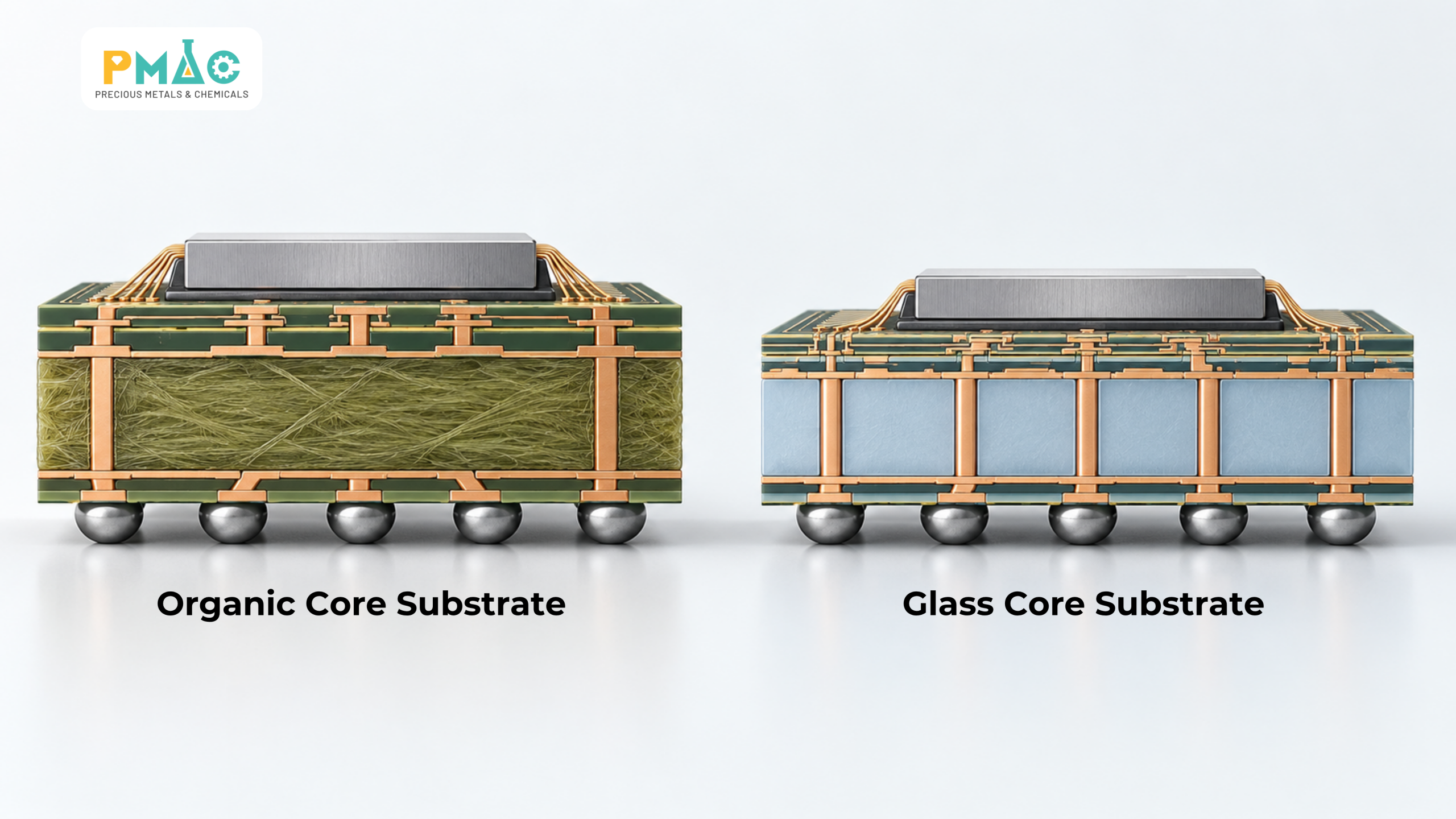
Figure 1. Comparison between organic-core package substrates and Glass Core Substrates
II. AI Chips Are Pushing Package Substrates Toward New Limits
Pressure on the substrate is increasing alongside the rise of heterogeneous integration. Rather than building an entire processor on a single very large monolithic die, the semiconductor industry is increasingly combining multiple dies with different functions within the same package. This is also the foundation of the chiplet architecture, in which individual functional blocks can be designed and manufactured separately before being integrated into a complete system.
HBM further increases this complexity. Multiple DRAM layers are stacked to form high-bandwidth memory and positioned close to the processor to shorten data-transfer paths. When a package contains a processor, multiple chiplets, and several HBM stacks, both the package area and the number of interconnections increase substantially. PMAC has discussed this technology in greater detail in What Is HBM?.
This trend can be clearly observed in TSMC’s CoWoS platform. The technology is designed to integrate logic chips, chiplets, and HBM in AI and high-performance computing systems, while continuing to scale toward larger package sizes.
The technical challenge is that packages need to become larger without sacrificing precision. As substrate area increases, thermal expansion, warpage, and layer-to-layer misalignment become increasingly difficult to control. The substrate material therefore moves beyond a purely mechanical role and becomes a direct factor in determining how far the chip architecture can scale.
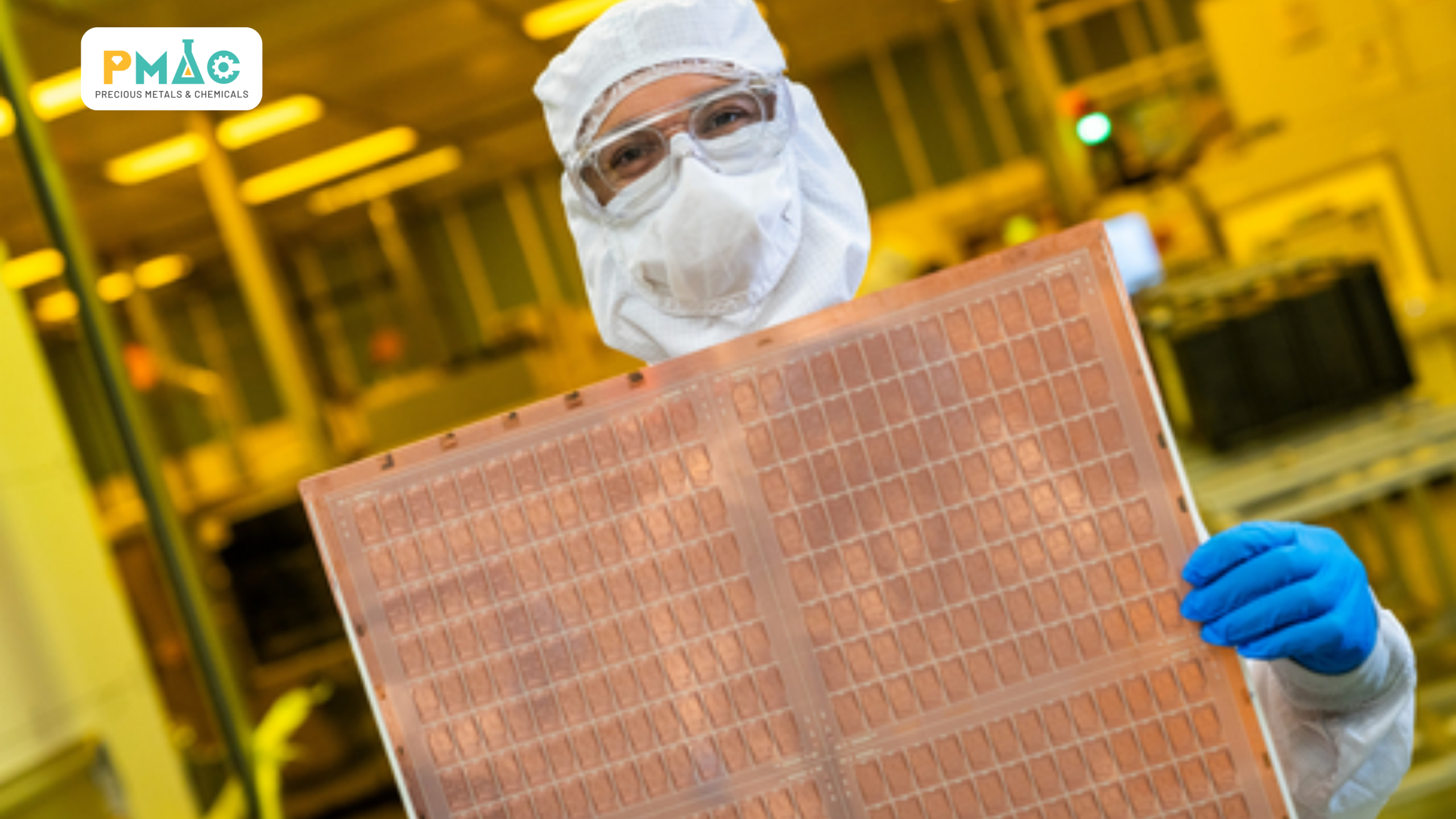
Figure 2. Key properties driving interest in glass for large AI packages
III. Flatness and Dimensional Stability Are Core Advantages of Glass
One of the most important advantages of glass is its ability to maintain geometric stability through thermal cycles. A semiconductor package typically combines silicon, copper, dielectric materials, and several other layers, each with its own coefficient of thermal expansion. If these differences are not properly controlled, accumulated stress can cause warpage and reduce the accuracy of subsequent manufacturing steps.
Corning offers semiconductor glass with different coefficients of thermal expansion, allowing materials to be selected according to the requirements of specific package structures. Glass also provides high stiffness, low electrical loss at high frequencies, and the ability to be manufactured as large panels or very thin sheets, creating additional design flexibility for complex packaging processes.
Flatness becomes particularly important as interconnect lines and connection pitches continue to shrink. Across a large package, small geometric deviations can accumulate into significant errors between distant areas. A more stable substrate improves layer-to-layer alignment and supports the formation of higher-density interconnect networks.
Intel states that its glass substrate platform can reduce pattern distortion by approximately 50% while providing the potential for up to an order-of-magnitude increase in interconnect density compared with organic substrate technologies under the conditions evaluated by the company. These figures apply to Intel’s own technology platform rather than to every Glass Core Substrate, but they illustrate the potential that greater material stability can provide for next-generation packages.
The value of glass therefore comes not from one isolated property, but from the combination of flatness, thermo-mechanical stability, electrical performance, and support for high-density interconnections. These characteristics become increasingly important as AI packages continue to grow in both size and complexity.
IV. TGV Turns Glass into Part of the Electrical Interconnect System
A highly flat and stable glass layer is still insufficient as a package substrate if power and signals cannot pass through it. This is the role of Through-Glass Via – TGV.
In principle, microvias are formed through the glass, after which their internal surfaces are treated and metallized to create electrical pathways between the two sides of the substrate. TGV therefore allows the glass layer to function not only as mechanical support but also as part of the electrical interconnect infrastructure inside the package.
Corning notes that glass is an insulating material with low electrical loss, particularly at high frequencies. Its adjustable coefficient of thermal expansion and ability to accommodate precise TGV structures make it suitable for interposers and other semiconductor packaging applications that require high interconnect density.
However, TGV is also one of the major technical challenges in Glass Core manufacturing. TrendForce notes that via formation requires tight control of laser energy to minimize dimensional variation and microcracking in the glass. As via dimensions continue to shrink, surface treatment and the formation of conductive metal layers inside the structures also become more difficult to control.
At this point, Glass Core shifts from being simply a glass material challenge to becoming a challenge involving the entire manufacturing process.
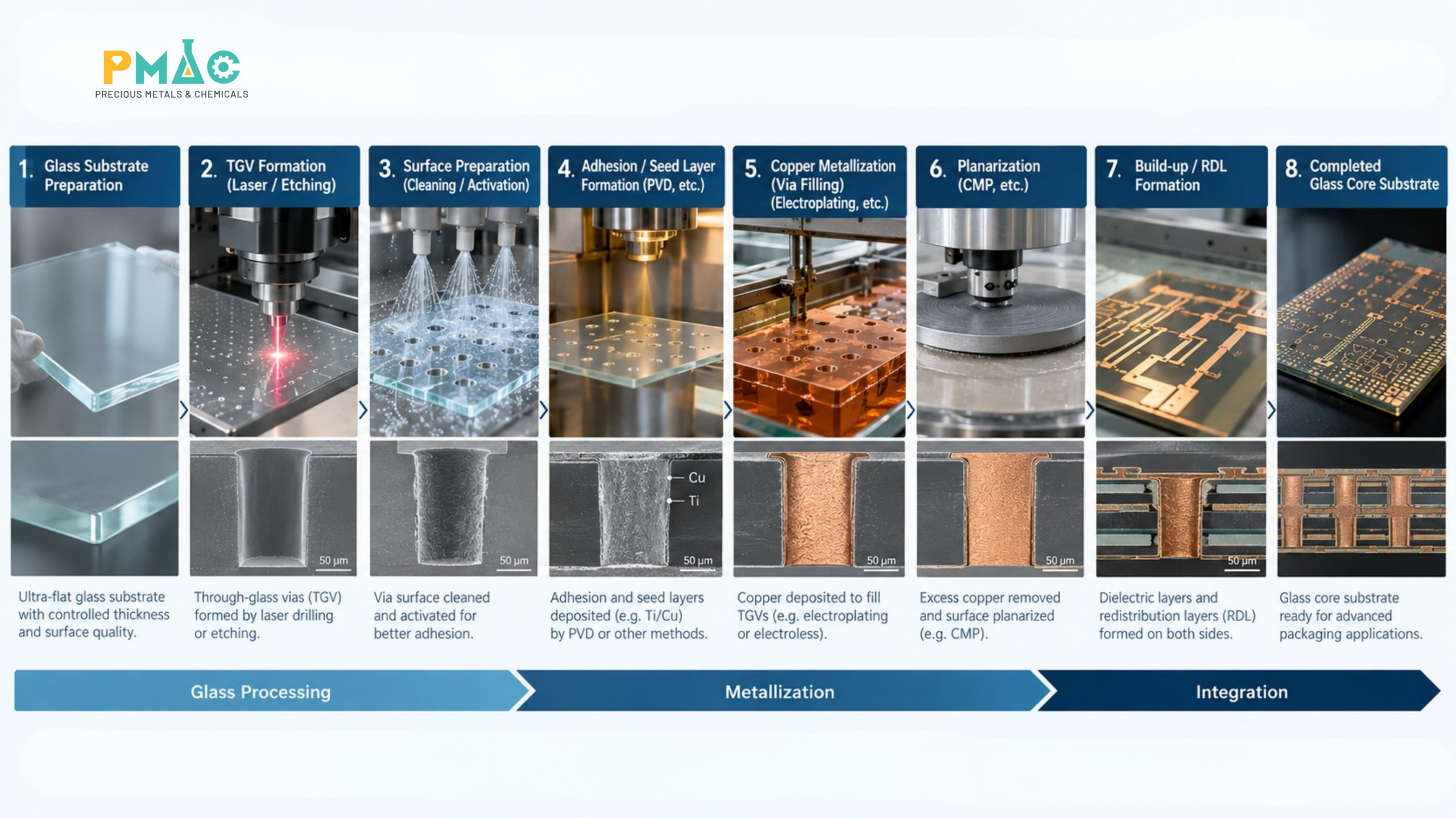
Figure 3. From Through-Glass Via formation to metallization in a Glass Core Substrate
V. Glass Core Creates New Requirements for Thin-Film Deposition, Metallization, and Metrology
Once TGVs have been formed, the holes must be converted into highly reliable electrical pathways. This requires a sequence of processes involving surface preparation, initial conductive layer formation, metallization, interconnect build-up, and precise control of surface geometry.
SEMI identifies TGV formation, metallization, build-up, dicing, and cracking as key bottlenecks in the current Glass Core manufacturing chain. This indicates that commercialization depends not only on the glass material itself, but also on whether multiple technology layers can operate reliably together within a single process.
During metallization, the uniformity and quality of the conductive layer directly influence resistance, interconnect durability, and TGV reliability. This is also where Glass Core intersects with technologies PMAC has previously discussed in semiconductor electroplating materials, where materials, surface conditions, and process control need to be evaluated as an integrated system rather than as isolated variables.
After metallization, measurement and process control become equally important. Manufacturers need to determine whether metal layers meet thickness requirements, whether the surface contains defects or geometric deviations, and whether the process remains consistent across production batches. Analysis and metrology therefore do not serve only as final inspection steps; they become integral to Glass Core process control.
This perspective also reflects how PMAC is developing its semiconductor capabilities: rather than treating materials, equipment, and metrology as separate product categories, PMAC places them in relation to each stage of the manufacturing process. This is an important distinction between simply identifying a technology trend and understanding the capabilities required to implement it in practice.
VI. Glass Core Expands the Design Space for Chiplets and HBM
The significance of Glass Core lies not simply in replacing an organic layer with glass, but in its ability to create additional design space for the entire package.
When an AI processor must continuously exchange data with multiple chiplets and HBM stacks, the substrate needs to accommodate an increasing number of signal paths within a limited area. If connection pitches cannot continue to shrink, or if the package cannot grow while maintaining geometric accuracy, further expansion of computing resources will eventually face physical constraints.
The dimensional stability of glass can help maintain high-density interconnect networks over a larger area, making it particularly relevant to multi-die systems that must operate as a unified architecture. This is also why Intel identifies AI, data centers, and high-performance graphics as some of the first markets suited to glass substrate technology.
In July 2026, Intel and Lens Technology announced further collaboration on glass-substrate-based packaging solutions. The partnership focuses on increasing interconnect density, performance, and energy efficiency for AI platforms, data centers, and specialized computing.
The key point is that packaging materials are becoming a direct part of the performance equation. As processing speeds within individual dies continue to increase, real system performance increasingly depends on how efficiently data can move between processors, chiplets, memory, and surrounding components.
VII. CoPoS Moves AI Packaging from Wafers Toward Larger Panels
The development of Glass Core is taking place alongside another shift in advanced packaging: moving part of the manufacturing process from round wafers to square or rectangular panels. This approach is gaining attention as AI packages become larger and manufacturers seek to use processing area more efficiently.
TrendForce reports that TSMC is developing Chip-on-Panel-on-Substrate – CoPoS around a standard panel format of 310 × 310 mm. The current roadmap identifies 2026 as an equipment and material validation phase, followed by pilot production in 2027 and a target for mass production beginning in the second half of 2028.
Square panels can use available area more efficiently than round wafers when accommodating very large packages. This creates additional room for more dies and HBM while providing a manufacturing path that better supports the continued scaling of AI systems.
However, CoPoS is not the same as Glass Core Substrate, nor has it replaced CoWoS. CoPoS describes a panel-level packaging approach, whereas Glass Core refers to a substrate material platform. CoWoS remains an important TSMC platform for AI and high-performance computing.
TrendForce currently distinguishes the two development paths relatively clearly: CoPoS is a near-term focus, while Glass Core is expected to represent a subsequent development direction, with large-scale commercialization potentially emerging after 2030.
The relationship among CoWoS, CoPoS, and Glass Core should therefore be understood as the evolution of advanced packaging across different technology layers, rather than as one technology directly replacing another.
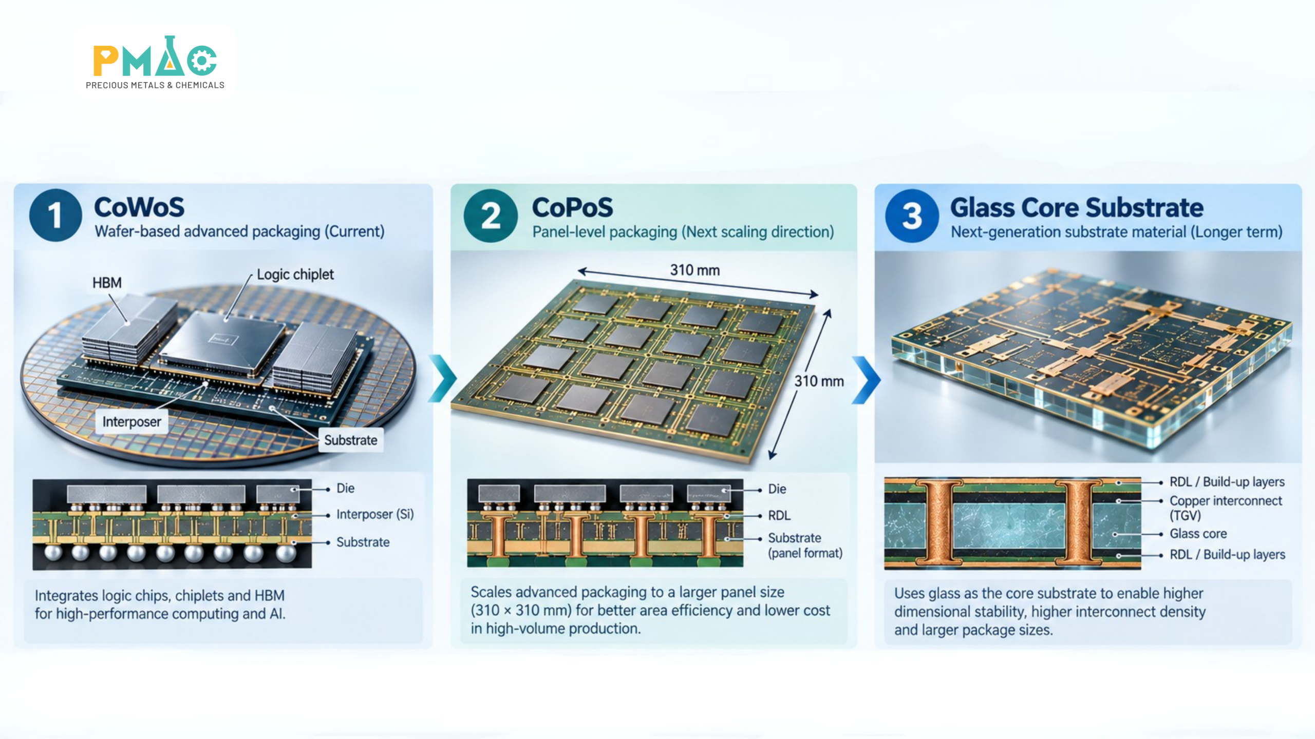
Figure 4. The relationship between CoWoS, CoPoS, and Glass Core Substrate in the AI packaging roadmap
VIII. The Economics of Glass Core Depend on the Entire Manufacturing Process
Glass Core is often discussed alongside expectations for lower AI packaging costs, particularly when combined with panel-level packaging. However, it would be inaccurate to assume that simply replacing an organic core with glass will automatically reduce package costs.
Part of the economic benefit comes from panel processing, where square or rectangular formats can use area more efficiently than round wafers for very large packages. Glass Core may support this model through its flatness and dimensional stability, but this represents only one component of the total cost structure.
Manufacturing cost also depends on TGV formation speed, metallization capability, production yield, build-up process stability, equipment costs, and the ability to operate consistently at industrial scale. SEMI also notes that the Glass Core market is still in an exploratory phase, with several manufacturing bottlenecks, standardization issues, and supply-chain readiness challenges yet to be fully resolved.
The benefits of Glass Core should therefore be evaluated at the level of the entire manufacturing system, rather than through a simple material-cost comparison between glass and organic cores. A new material creates economic value only when its technical advantages can be translated into stable production output and sufficiently high yields.
IX. TGV, Warpage, and Yield Remain Key Barriers to Commercialization
Although glass offers several characteristics suited to next-generation packages, a significant gap remains between successful prototypes and stable high-volume production. The main challenge is maintaining the same degree of precision across very large production volumes.
TGV provides a clear example. Via dimensions must remain consistent, while the surrounding glass must avoid microcracks that could propagate under thermal stress. The metal formed inside each via must also be continuous and stable enough to preserve electrical performance throughout the device lifecycle.
Flatness becomes more difficult to maintain as panel size increases. Glass Core has an inherent advantage in geometric stability, but maintaining very high precision across large areas still requires equally advanced equipment and process control. Surface deviations can affect lithography and layer alignment, ultimately reducing manufacturing yield.
In addition, glass does not operate in isolation. It must be integrated with copper, dielectric materials, and multiple other layers with different thermal properties. A more stable glass core therefore does not automatically eliminate package warpage. The engineering challenge remains the simultaneous optimization of materials, equipment, structures, and processes.
X. Glass Core Is Moving from Material Research Toward Supply-Chain Development
One indication that Glass Core is moving closer to commercialization is the growing range of companies participating in its development. The market is no longer limited to materials research groups but is beginning to form a broader network of glass suppliers, substrate manufacturers, chemical suppliers, equipment providers, process-technology companies, and packaging manufacturers.
Intel was one of the earlier companies to publicly develop glass substrate technology. After more than a decade of research, the company is gradually shifting toward building a production ecosystem through partners such as Lens Technology, combining advanced packaging capabilities with precision glass-processing expertise.
Samsung Electro-Mechanics is moving in a similar direction. Its agreement with Sumitomo Chemical Group focuses on developing Glass Core manufacturing capabilities for next-generation package substrates, reflecting a transition from material experimentation toward preparation for industrial production.
From an industry-wide perspective, SEMI considers Glass Core to remain in an emerging stage, with limited production potentially beginning around 2028 for selected applications. Actual progress, however, will continue to depend heavily on technology validation, supply-chain readiness, and the establishment of common standards.
These developments indicate that glass has moved beyond the stage of being an isolated research concept, although it has not yet become a default material across the industry. Commercial adoption is likely to begin in applications where the technical advantages of Glass Core are significant enough to justify the complexity and cost of implementing a new manufacturing process.
XI. Glass Core Reflects a Broader Shift in the AI Chip Race
Glass Core Substrate is important not because glass has become a perfect material capable of replacing every organic substrate. Most mainstream semiconductor products still do not require package sizes or interconnect densities high enough to create a clear economic advantage for the technology.
The benefits of glass are more likely to emerge in AI chips, AI accelerators, data centers, and high-performance computing, where multiple chiplets and HBM stacks need to be connected within the same package. As component counts increase, the substrate is no longer merely a mechanical base but becomes a direct part of the system’s performance architecture.
Glass Core therefore reflects a broader shift within the semiconductor industry: performance is no longer determined solely by the transistors inside the chip. Materials, interconnect structures, metallization, metrology, and packaging technologies increasingly determine how far an entire system can continue to scale.
For companies seeking deeper participation in the semiconductor supply chain, this trend also shows that opportunities extend beyond chip design or wafer fabrication. Materials, chemicals, surface treatment, equipment, analysis, and metrology are becoming increasingly important links as advanced packaging continues to evolve.
This is also the direction PMAC is developing within its industrial and technology ecosystem: connecting materials, equipment, analysis and metrology, and technical support around the actual requirements of individual manufacturing processes rather than building a semiconductor portfolio around isolated products.
Follow PMAC for more insights into semiconductor packaging, testing, and materials.
PMAC Joint Stock Company
Ho Chi Minh City Office:
4th Floor, HUTECH Building, D1 Road, Saigon Hi-Tech Park, Tang Nhon Phu Ward, Ho Chi Minh City, Vietnam
Hanoi Office:
22B O2, Linh Dam Peninsula, Hoang Liet Ward, Hanoi, Vietnam
Hotline: +84 387 235 878
Facebook: PMAC