

Once again, PMAC has chosen not to be satisfied with the strong achievements it has already made. The new fiscal year continues with a series of Saturday morning training sessions, focusing on a topic that is attracting significant attention across the technology and industrial sectors: semiconductor technology.
This is not the first time a new technology has generated strong market interest. But semiconductors are different from many short-term trends. Behind a chip only a few millimeters in size lies decades of accumulated knowledge, billion-dollar production lines, and a global network spanning design, materials, equipment, software, fabrication, packaging, testing, and scientific research.
PMAC is also not approaching this field as a complete newcomer. For many years, the company has operated in the electronics sector, supplying products and solutions to a wide range of customers, including companies involved in semiconductor manufacturing. However, experience accumulated through individual products and projects is different from establishing a formal, proactive, and systematic strategic direction.
As technology evolves rapidly and global supply chains continue to be restructured, this is the right time for PMAC to look at the broader picture, connect its existing capabilities, and define more clearly its long-term role in the semiconductor ecosystem.
I. When a “Hot” Topic Requires a Cool-Headed Approach
Semiconductors are appearing increasingly often in Vietnam’s national strategies, training programs, investment forums, and industrial development plans. According to the Strategy for the Development of Vietnam’s Semiconductor Industry to 2030, with a Vision to 2050, Vietnam aims to develop capabilities in design, manufacturing, packaging, testing, electronics, and human resources under the following formula:
C = SET + 1
Where:
C: Chip;
S: Specialized – specialized chips;
E: Electronics – electronics industry;
T: Talent – human resources;
+1: Vietnam – a new safe destination for the global semiconductor supply chain.
However, there is still a significant gap between identifying an industry as a national priority and actually building a complete technology ecosystem. The semiconductor industry cannot be developed simply by installing equipment inside a factory. Every stage requires specialized talent, process control capabilities, stable material supplies, stringent quality standards, and coordination among companies across multiple fields.
For this reason, PMAC does not want its team to take away only a collection of technical terms from the training series. More importantly, the objective is to develop the ability to view the semiconductor industry as an interconnected system rather than a collection of isolated processes or an opportunity defined only by impressive investment figures.
II. From Silicon Atoms to the Switches of the Digital World
Discussions about semiconductors often quickly shift toward billion-dollar fabs, process nodes measured in only a few nanometers, or processors designed for artificial intelligence. However, to understand the fundamentals of the industry, PMAC’s first training session began at a much smaller scale: the silicon atom.

Silicon Atom
Silicon is a semiconductor material whose electrical conductivity lies between that of a conductor and an insulator. This property is not fixed. It can be modified by adding carefully controlled amounts of other elements through a process known as doping.
Starting from high-purity silicon, doping creates N-type and P-type semiconductor materials with different electrical characteristics. When these regions are combined in the appropriate structure, electrical current can be controlled to switch, amplify, or process signals.
This forms the basis of the transistor – the microscopic electronic switches behind most digital devices today. Transistor patterns and interconnections are built layer by layer on silicon wafers through repeated processes of adding, shaping, and removing materials.
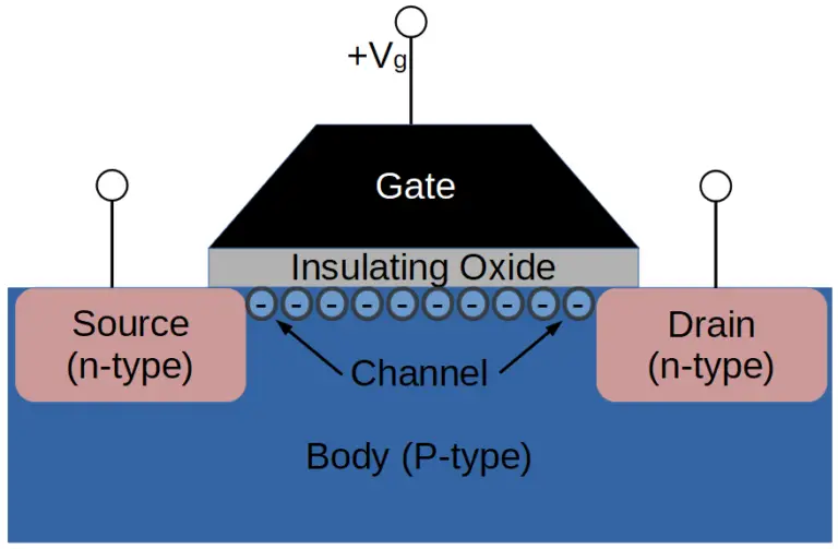
Structure of a Transistor
What is remarkable is not only the extremely small size of a transistor, but also the level of precision required to manufacture it. When component behavior depends on material composition at the atomic scale, seemingly insignificant changes in impurities, surface conditions, or processing environments can affect the final result.
This is also an important connection for the PMAC team. In precious metals, technical chemicals, and advanced materials, quality is not defined solely by the product name or the headline specifications listed in a catalogue. Purity, batch-to-batch consistency, storage conditions, technical documentation, and traceability must all be considered as part of an integrated system.
III. When Transistors Change, the Entire Ecosystem Must Change With Them
A single transistor can perform only a very basic function. But when millions or billions of transistors are arranged and interconnected within the same integrated circuit, they form processors, memory devices, sensors, and many other complex electronic systems.
The development of the semiconductor industry has therefore been closely linked to efforts to place more transistors within the same area while improving performance and power efficiency. During the training session, PMAC’s team explored the evolution of transistor structures from traditional planar designs to FinFET and Gate-All-Around (GAA).
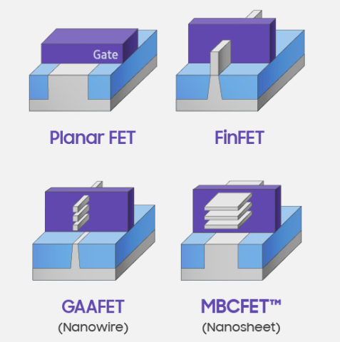
Transistor Structures
In a planar transistor, the conduction channel lies relatively flat on the wafer surface. In a FinFET, the channel is raised into a fin-like structure, allowing the gate to control it from multiple sides. With GAA, the gate surrounds the channel, improving current control as transistor dimensions continue to shrink. Samsung describes the transition from planar to FinFET and GAA as a continuous effort to improve current control at the transistor level.
On a diagram, these developments may appear to be simple changes in geometry. In manufacturing, however, every new transistor generation creates different requirements for materials, thin films, equipment, precision, and inspection methods.
A change at the smallest structural level of a chip can therefore trigger changes across multiple layers of the supply chain. Keeping up with semiconductor technology cannot stop at learning the names of the latest processors. Companies must understand how the underlying technologies are changing and what new requirements those changes create for the broader ecosystem.
IV. Silicon Wafer: The Foundation of a Multi-Layer System
Before transistors can be formed, the semiconductor industry requires a substrate with extremely high purity and uniformity: the silicon wafer.
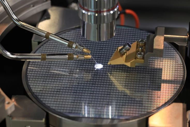
Silicon wafer
Silicon may originate from naturally occurring silica, but before it can become a wafer suitable for chip fabrication, the material must undergo multiple stages of purification, crystal growth, slicing, and surface treatment. Only then can the wafer enter the processes used to build transistor patterns and interconnect structures layer by layer.
The journey from raw material to wafer illustrates an important principle of the semiconductor industry: the material itself is only the starting point. Technological value lies in the ability to control that material consistently and reproducibly across a long sequence of processes.
Each new layer must be positioned precisely on top of the structures formed before it. A deviation at one stage may continue to affect subsequent processes, even if it cannot be detected visually. Semiconductor manufacturing therefore depends heavily on measurement equipment, environmental control systems, and the ability to maintain material consistency.
For PMAC, this way of thinking is not entirely unfamiliar. Years of working with precious metals, technical chemicals, and surface technologies have taught the team that a solution creates real value only when it matches the substrate material, operating conditions, and actual quality requirements.
However, similarities in mindset do not mean that experience from one industry can simply be transferred unchanged into semiconductors. The semiconductor sector has its own standards, qualification methods, and levels of process control. The purpose of the training is therefore not to reach quick conclusions, but to help PMAC identify which capabilities it already has and which standards still need to be strengthened.
V. Technology Nodes Are Not the Only Measure of a Chip
Terms such as 90 nm, 28 nm, 7 nm, and below 5 nm are frequently mentioned when discussing semiconductors. However, node size alone cannot fully represent the capability or value of a technology.

Development of Technology Nodes – Source: TSMC
Leading-edge nodes are often selected for applications requiring high computing density and energy efficiency, such as artificial intelligence, high-performance computing, and premium mobile devices. Meanwhile, many mature nodes remain critical in automobiles, industrial equipment, sensors, microcontrollers, analog circuits, networking equipment, and power management systems.
The most appropriate technology is therefore not necessarily the one with the smallest nanometer number. The choice also depends on application requirements, performance, reliability, production volume, power consumption, and manufacturing cost.
This understanding helps PMAC avoid viewing the semiconductor market as a race with only one direction. Behind the most advanced technologies lies a broad ecosystem of different process generations, product categories, and material requirements. Understanding the technology landscape requires seeing both the high-profile innovations attracting attention and the mature platforms that continue to power most modern electronic devices.
VI. A Chip Is the Result of an Entire Ecosystem
From silicon atoms, transistors, and wafers, the training expanded into how the semiconductor value chain is structured. A chip does not necessarily have to be designed, manufactured, and commercialized by the same company. Some companies focus on design without owning fabrication facilities. Foundries manufacture chips based on customer designs. Other companies operate under the IDM model, combining both design and manufacturing. ASML and Intel both describe this division of roles as a defining characteristic of the modern semiconductor industry.
Surrounding these companies is another network of wafer suppliers, manufacturing equipment providers, chemical and material suppliers, design software companies, measurement systems, and packaging and testing service providers.
The semiconductor “map” is therefore not a simple linear chain running from raw material to final product. It is an interdependent network in which a technological change in one layer can generate new requirements for companies across many other layers.
Understanding this structure is particularly important for PMAC. The company has many years of experience in the electronics sector and has supplied products and solutions to semiconductor-related customers. However, moving from individual experiences toward a systematic strategy requires placing each activity within the broader context of the industry.
The first question is therefore not simply which process PMAC should participate in. More fundamental questions must come first: Where is technology moving? How is the value chain being reorganized? And which new standards will shape relationships between customers, suppliers, and technology partners in the future?
VII. PMAC’s Existing Foundation and the Standards That Still Need to Be Strengthened
Over many years of operation, PMAC has built experience in precious metals, precious metal chemicals, surface technologies, analytical equipment, and technical solutions for the electronics industry. The company has also served customers involved in semiconductor manufacturing.
This foundation has taught PMAC that the quality of a technical solution does not depend only on the product name or published specifications. Material origin, purity, batch consistency, technical documentation, traceability, and supporting services all influence actual performance.
This is also how PMAC approaches electroplating chemicals for the electronics industry: solutions should be selected based on substrate materials, surface requirements, production-line conditions, and quality objectives rather than simply choosing from a predefined catalogue. Readers can learn more in How to Select the Right Electroplating Chemicals for a Production Line and Applications of Electroplating Chemicals in Electronics and Precision Engineering.
However, having an existing foundation does not mean that every requirement of the semiconductor industry has already been addressed.
Semiconductors have their own technical standards, qualification procedures, and risk-control mechanisms. PMAC’s task is therefore not simply to transfer existing capabilities from one field into another, but to reassess each capability in a new context: which capabilities are already suitable, which need to be upgraded, and which gaps must be filled through knowledge, technology, or international partnerships. This is the mindset behind the Saturday morning training series.
VIII. Defining PMAC’s Role Through a More Structured Approach
Choosing not to be satisfied with past achievements also means refusing to let experience become a reason to stop asking questions. PMAC’s first semiconductor technology training session returned to the fundamentals: silicon, transistors, wafers, interconnect layers, technology nodes, and more. But the greatest value does not lie in the number of technical terms introduced.
The real value lies in enabling the team to view years of accumulated activities through a more complete framework. From here, PMAC will not simply continue supplying individual products and solutions for isolated needs. The company is beginning to connect market experience, technical capabilities, its partner network, and technology knowledge into a more proactive, consistent, and long-term direction.
We will continue to update our knowledge, strengthen technical capabilities, and connect our experience in precious metals, chemicals, and surface technologies with the increasingly demanding requirements of the electronics and semiconductor industries.
Explore more about PMAC’s capabilities and areas of expertise or contact the PMAC team to discuss materials, chemicals, and technical solutions for your business.
PMAC Joint Stock Company
Ho Chi Minh City Office:
4th Floor, HUTECH Building, D1 Road, Saigon Hi-Tech Park, Tang Nhon Phu Ward, Ho Chi Minh City, Vietnam
Hanoi Office:
22B O2, Linh Dam Peninsula, Hoang Liet Ward, Hanoi, Vietnam
Hotline: +84 387 235 878
Facebook: PMAC