

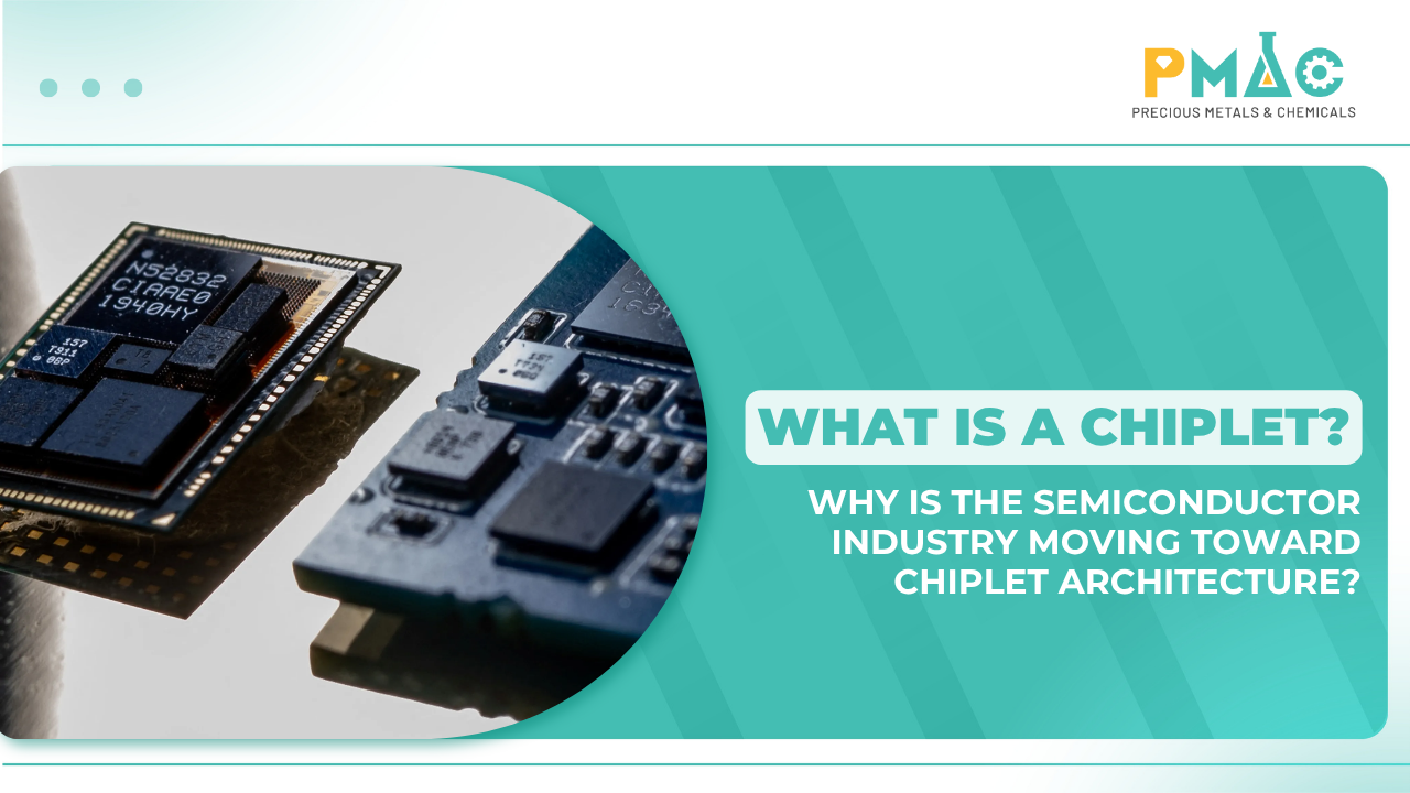
For decades, one of the most common ways to increase chip performance has been to integrate more and more transistors onto a single die. However, as processors become larger, more complex, and increasingly designed for workloads such as AI, HPC, and data centers, monolithic chip architectures are beginning to face challenges related to die size, design cost, scalability, and manufacturing.
An alternative approach that is attracting growing attention is the chiplet.
Instead of building an entire processor on one large die, designers can divide the system into multiple smaller dies or functional blocks and then integrate them within the same package. AMD is one of the most prominent examples, using chiplet architecture in its Zen and EPYC processors, while Intel is also developing a chiplet ecosystem alongside packaging technologies such as EMIB and Foveros.
This represents an important shift in chip design thinking:
Instead of simply trying to build a larger die, the semiconductor industry is increasingly focused on building a better system from multiple efficiently connected dies.
I. Chiplet
1. What Is a Chiplet?
A chiplet can be understood as a processing module or die that performs a specific part of a system’s overall function. Multiple chiplets can then be integrated within the same package to create a complete processor.
This concept is closely associated with chiplet architecture or chiplet design, in which multiple chiplets are connected and designed to operate as a unified system.
2. What Does a Chiplet System Include?
A chiplet-based system may include:
- Compute/CPU Core Chiplet: contains processing cores.
- I/O Chiplet: handles communication with memory, PCIe, or external devices.
- Memory Controller: manages communication with memory.
- Cache Chiplet: provides cache memory.
- Accelerator Chiplet: handles AI, graphics, or other specialized workloads.
Think of a chip as a LEGO set. In a monolithic design, almost the entire product is built as one large block. With chiplets, designers can combine different functional “LEGO pieces” to create a complete system.
II. How Are Chiplets Different From Monolithic Chips?
To understand why chiplets are gaining attention, it helps to compare them with monolithic chips.
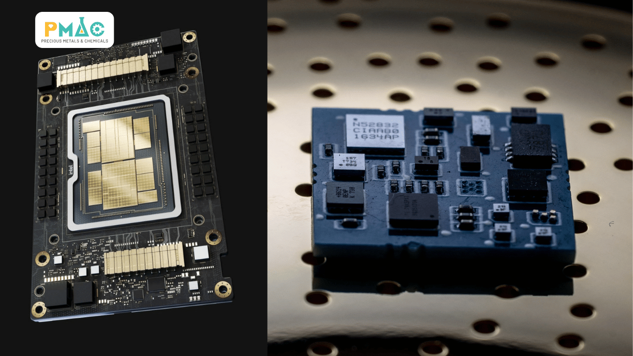
Figure 1: Differences between chiplets and monolithic chips
1. Monolithic Chips
In a monolithic architecture, most processor functions are integrated onto a single large silicon die.
The structure can be visualized as:
CPU + Cache + I/O + Memory Controller → One Die
One advantage of this approach is that components on the same die can communicate through very short, high-density, low-latency connections.
However, as the die becomes larger, both design and manufacturing become more complex.
2. Chiplet
With chiplet architecture, the system is divided into multiple dies:
Compute Chiplet + Compute Chiplet + I/O Chiplet + Cache/Accelerator → One Package
These dies communicate through dedicated die-to-die interconnects designed for high-speed data transfer.
3. Chiplet vs. Monolithic Chip
| Criteria | Monolithic Chip | Chiplet |
|---|---|---|
| Architecture | One large die | Multiple dies/chiplets |
| Design | Fully integrated | Modular |
| Reuse | More limited | Potentially higher |
| Scalability | More difficult as die size increases | Chiplets can be added or changed |
| Process node flexibility | More limited | More flexible |
| Interconnect | Mostly within the die | Requires die-to-die interconnects |
| Packaging | Relatively simpler | More complex |
| Testing | Focused mainly on the die | Must manage multiple dies and the package |
| Cost | Depends on design and node | Can optimize some areas, but packaging costs increase |
The key point is that chiplets are not automatically cheaper or faster than monolithic chips.
Actual performance depends on architecture, process node, interconnect technology, package design, yield, production volume, and system requirements.
The main advantages of chiplets lie in flexibility and scalability.
III. Why Are Chipmakers Moving Toward Modular Designs?
The semiconductor industry is not completely abandoning monolithic chips. In reality, both approaches continue to coexist.
However, chiplets become increasingly attractive as system scale and integration requirements grow. There are at least five major reasons.
1. Reducing the Challenges of Very Large Dies
A large die containing an entire system becomes increasingly difficult to design and manufacture as transistor counts rise.
Chiplets make it possible to divide functions into smaller dies.
For example, instead of creating one very large die containing both compute and I/O functions, designers can separate them into:
Compute Die + I/O Die
2. Improving Scalability
One of the clearest advantages of chiplet architecture is the ability to create multiple product configurations from similar building blocks.
A designer may use the same compute chiplet as a foundation, then vary the number of chiplets or combine them with different I/O dies to create different products. This is particularly useful for CPUs and accelerators serving multiple market segments.
AMD has stated that chiplet architecture allows its processors to scale by adding processing building blocks within the package.
3. Reusing IP and Chiplets
A well-designed chiplet can become a reusable building block across multiple products. This differs from developing an entirely new die for every product configuration.
However, high levels of reuse require compatibility across interfaces, power delivery, thermal requirements, and overall system design. Therefore, chiplet reuse is not only a silicon design challenge; it is also an ecosystem challenge.
4. Combining Multiple Process Nodes
This is one of the most important technical advantages. Not every component in a system needs to use the most advanced process node. Compute logic may benefit significantly from a leading-edge node, while I/O, analog functions, or certain control circuits may not require the same technology.
With chiplet architecture, different components can be developed and manufactured using the process technologies best suited to their functions, then integrated within the same package. This is the essence of heterogeneous integration – combining components with different functions, technologies, or process nodes within one system.
Applied Materials also describes heterogeneous integration as an approach that enables chips with different technologies, functions, and sizes to be integrated within the same package.
>>> Reference: Cutting-Edge Process Technologies for Data Center
5. Supporting AI and HPC
AI accelerators and High Performance Computing – HPC systems are creating enormous demand for compute power, memory capacity, bandwidth, and connectivity.
A modern AI system does not simply require more computation. It must also move enormous volumes of data between compute and memory with very low latency.
This is why chiplets are becoming increasingly closely connected with advanced packaging and HBM.
IV. How Are Chiplets Related to Advanced Packaging?
If chiplets are the “LEGO blocks,” then advanced packaging is the platform that allows those blocks to be assembled into an efficient working system. This distinction is important.
Chiplets cannot deliver their full benefits if the dies are merely placed next to each other but communicate slowly, consume too much power, or occupy too much area. That is why the semiconductor industry has developed advanced packaging technologies that reduce the distance between dies while increasing interconnect density.
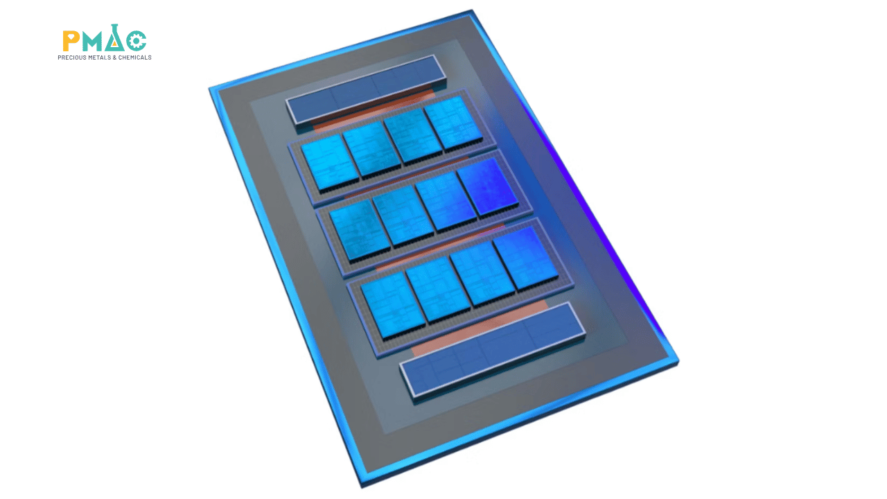
Figure 2: Chiplet architecture integrating multiple dies within a single package
Several important technologies include:
1. 2.5D Packaging
In 2.5D packaging, multiple dies can be placed side by side on an interposer or another high-density interconnect platform.
A prominent example is TSMC CoWoS, where a silicon interposer can connect multiple logic chiplets and HBM stacks within a single package. TSMC currently describes CoWoS-S as a system integration solution for HPC that combines large silicon interposers, logic chiplets, and HBM.
2. Interposer
An interposer is an intermediate layer containing a high-density interconnect network positioned between the dies and the package substrate below.
Instead of routing every connection directly down to the package substrate, an interposer enables shorter and denser connections between dies.
3. 3D Packaging
Unlike 2.5D packaging, 3D packaging stacks dies vertically.
The goal is to shorten the distance between layers and increase integration density.
Intel has developed packaging technologies such as Foveros, including 3D stacking and high-density die-to-die interconnect approaches. Intel also combines EMIB and Foveros in 3.5D configurations for complex heterogeneous systems.
4. TSV
TSV – Through-Silicon Via refers to vertical electrical connections that pass through silicon.
TSVs are particularly important in 3D structures, where signals and power must move between stacked layers.
5. Hybrid Bonding
Hybrid bonding is a method of directly bonding die or wafer surfaces, typically combining metal structures with dielectric materials. One of its main objectives is to create higher-density die-to-die interconnects with smaller spacing.
Recent research from imec continues to focus on fine-pitch RDL and die-to-wafer hybrid bonding for high-density chip-to-chip systems. In simple terms:
Chiplet → Requires high-speed interconnects → Requires advanced packaging → Requires interposer/RDL/TSV/hybrid bonding → Creates a high-density integrated system.
V. Challenges of Chiplet Architecture
Chiplets offer many advantages, but they are not a “magic button.” A multi-die system also creates a new set of challenges.
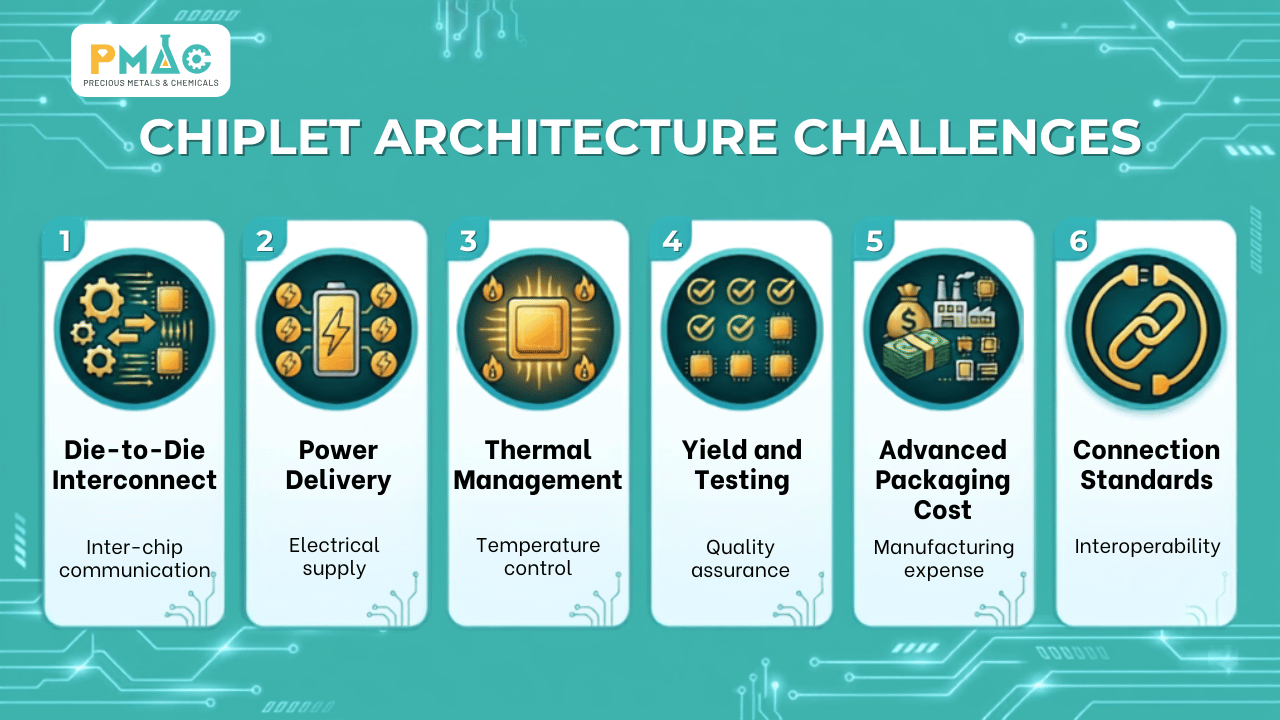
Figure 3: Challenges of chiplet architecture
1. Die-to-Die Communication
Chiplets must exchange data at high speed, with low latency and reasonable power consumption.
If the interconnect is not efficient enough, some of the benefits of dividing the system into smaller dies may be lost.
This is why standards and interfaces specifically designed for chiplets are becoming increasingly important.
2. Power Delivery
More chiplets mean power must be supplied and managed across multiple components within the same package. Power delivery design therefore becomes more complex.
3. Thermal Management
When multiple dies operate within one package, heat can become concentrated in particular areas. The challenge becomes even greater with 3D packaging because multiple silicon layers are stacked vertically.
4. Yield and Testing
A chiplet-based system consists of multiple dies, which means testing must also account for more individual components. Manufacturers therefore need to consider:
Die yield → Assembly yield → Package yield → System yield
An individual chiplet may perform correctly, while the full package must still ensure that every integrated component functions properly after assembly.
5. Advanced Packaging Cost
Chiplets may provide design and silicon manufacturing advantages in some cases, but advanced packaging increases overall system complexity.
Interposers, TSVs, RDL, microbumps, hybrid bonding, package testing, and thermal management can all increase costs.
6. Interconnect Standards
A truly flexible chiplet ecosystem requires interoperability between chiplets from different sources.
This is why UCIe – Universal Chiplet Interconnect Express has become an important development.
According to the UCIe Consortium, UCIe 3.0 was released on August 5, 2025, supporting data rates of 48 GT/s and 64 GT/s while adding improvements in management, power efficiency, and topology for chiplet-based systems. UCIe 3.0 is also backward compatible with previous versions.
This shows that chiplets are gradually evolving from proprietary design approaches used by individual companies into a broader ecosystem that requires common interconnect standards.
VI. Chiplets and the Future of the Semiconductor Industry
As AI models become larger, demand for computing power and memory bandwidth continues to increase. This creates a connected chain of requirements:
More Compute → Higher Memory Bandwidth → Faster Interconnects → More Complex Packages → Greater Need for Heterogeneous Integration
The future of chiplets therefore depends on much more than simply designing additional dies. It increasingly depends on the ability to combine:
Chiplets + HBM + Advanced Packaging + High-Speed Interconnects + Thermal Management
In other words, system performance is no longer determined solely by the transistors inside each die. It increasingly depends on how effectively the dies communicate with one another. This is why packaging is evolving from simply “packaging a chip” into a fundamental part of system architecture
VII. Chiplets and the Future of Modular Chip Design
The development of chiplets reflects a broader change in how the semiconductor industry defines “a chip.” In the past, the main focus was on transistors and individual dies.
Today, for high-performance systems, the central question is increasingly: How can multiple different dies operate as a single system while maintaining high performance, reasonable power consumption, and sufficient reliability?
Chiplets provide a modular approach to solving this problem. Advanced packaging provides the integration platform. Interposers, RDL, TSVs, and hybrid bonding increase interconnect density. HBM addresses memory bandwidth requirements.
UCIe opens the way toward a more standardized chiplet interconnect ecosystem. And material technologies, deposition, electroplating, and surface treatment help form the physical structures required to connect all of these components. Therefore, chiplets are not simply about splitting one chip into multiple smaller pieces. They represent a shift from “design a chip” to “design a system in package.”
Conclusion
Chiplets are becoming one of the most important directions in modern semiconductor design because they allow designers to move from a monolithic die toward a modular architecture that can scale more easily and integrate multiple technologies.
This is particularly important for AI and HPC, where growing demand for compute power, memory bandwidth, and I/O makes chiplets increasingly interconnected with HBM, advanced packaging, 2.5D/3D integration, and high-speed die-to-die interconnects.
However, chiplets require more than good silicon design. The overall system also needs an advanced packaging platform, sufficiently fast interconnects, effective thermal management, and highly precise manufacturing processes.
Within this ecosystem, deposition, electroplating, and surface treatment technologies play an important role at the material and physical interconnect level, helping form RDL, TSV, copper pillars, and other metal structures used in advanced packaging.
PMAC is steadily expanding its surface technology consulting capabilities for the electronics and semiconductor industries, connecting international materials and technology solutions with practical implementation needs in Vietnam.
Follow PMAC for more insights into semiconductor packaging, testing, and materials.
PMAC Joint Stock Company
Ho Chi Minh City Office:
4th Floor, HUTECH Building, D1 Road, Saigon Hi-Tech Park, Tang Nhon Phu Ward, Ho Chi Minh City, Vietnam
Hanoi Office:
22B O2, Linh Dam Peninsula, Hoang Liet Ward, Hanoi, Vietnam
Hotline: +84 387 235 878
Facebook: PMAC