

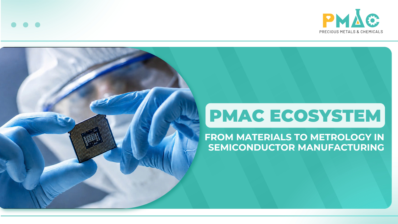
A semiconductor is a material whose electrical conductivity can be controlled, making it possible to create transistors and integrated circuits used in smartphones, computers, automobiles, industrial equipment, and most modern electronic systems. Silicon remains the most widely used semiconductor material, while materials such as SiC and GaN are increasingly applied where higher power, frequency, or thermal performance is required.
However, turning a semiconductor material into a finished chip requires a highly complex chain of technologies. The process typically begins with a wafer as the base material. On the wafer surface, multiple material layers are deposited, processed, patterned, and interconnected to form electronic structures. The chip then goes through dicing, assembly, packaging, testing, and metrology before it can be integrated into a final product.
The overall process can be viewed as a simple sequence: substrates → materials and chemicals → wafer processing equipment → assembly and packaging → analysis and metrology → automation. This is also how PMAC is developing its semiconductor portfolio—not around isolated products, but around interconnected technology layers that directly support different stages of semiconductor manufacturing.
I. What Are Semiconductor Substrates?
A semiconductor substrate is the base material on which the electronic structures of a chip are formed. It is typically manufactured as a thin disc known as a wafer. On the wafer surface, manufacturers progressively build material layers and circuit structures before the wafer is eventually diced into individual chips.
In this article, “substrate” refers to the base material used in semiconductor fabrication, rather than the package substrate used during the later packaging stage. PMAC is currently developing a portfolio that includes Silicon, SOI, SiC, GaN, as well as wafers for testing, inspection, and reclaim applications.
The choice of substrate depends on the type of device and its operating requirements. Silicon is suitable for most conventional semiconductor applications, while SiC and GaN are increasingly considered for applications requiring higher voltage, power, frequency, or thermal performance. Within the industry, SEMI also develops dedicated standards for different semiconductor materials and wafers, including SiC and GaN wafers.
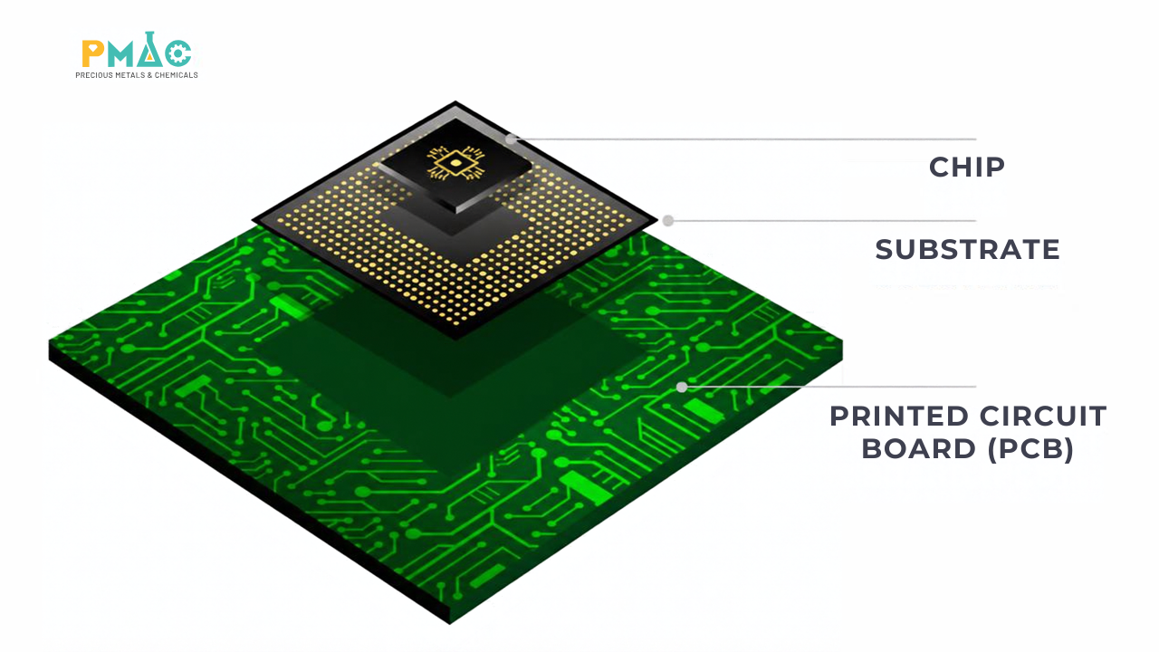
Figure 1: What Are Semiconductor Substrates?
I. What Do Semiconductor Materials and Chemicals Include?
Once the appropriate wafer has been selected, manufacturers must continuously add, remove, or modify extremely thin material layers on its surface. Technologies such as PVD, CVD, and ALD are used for thin-film deposition; photolithography and etching form patterns and structures; ion implantation modifies the electrical properties of materials; cleaning helps control contamination; while CMP is used to planarize the surface before subsequent layers are processed.
PMAC is expanding its semiconductor materials portfolio from PVD deposition materials and CVD/ALD precursors to electroplating materials, bonding materials, die-attach materials, high-purity chemicals, lithography materials, and CMP consumables.
Among these, semiconductor electroplating is one area that clearly builds on PMAC’s existing expertise in precious metals, chemicals, and surface technologies. In semiconductor devices, even extremely thin metallic layers can directly affect electrical conductivity, contact reliability, and overall device stability.
Because these process steps are interconnected and dependent on one another, semiconductor materials cannot be selected solely based on composition or individual specifications. Purity, batch-to-batch consistency, compatibility with equipment, and actual operating conditions can all influence downstream process results.
III. What Technologies Are Used in Semiconductor Manufacturing Equipment?
If materials are the inputs of the process, equipment is what directly creates and modifies structures on the wafer. Each manufacturing step requires a different group of technologies and a very high level of process control.
PMAC is expanding its semiconductor materials portfolio from PVD deposition materials and CVD/ALD precursors to electroplating materials, bonding materials, die-attach materials, high-purity chemicals, lithography materials, and CMP consumables.
This area also builds strongly on PMAC’s existing experience in precious metals, chemicals, and semiconductor electroplating materials, particularly in applications that require precise control of metal layer quality and process stability.
>> Learn more: Semiconductor Electroplating Materials at PMAC.
However, semiconductor manufacturing involves significantly higher control requirements: even very small levels of contamination, batch-to-batch variation, or compositional deviation can affect downstream process results. Materials therefore need not only to meet specifications, but also to be compatible with the equipment and actual manufacturing conditions.
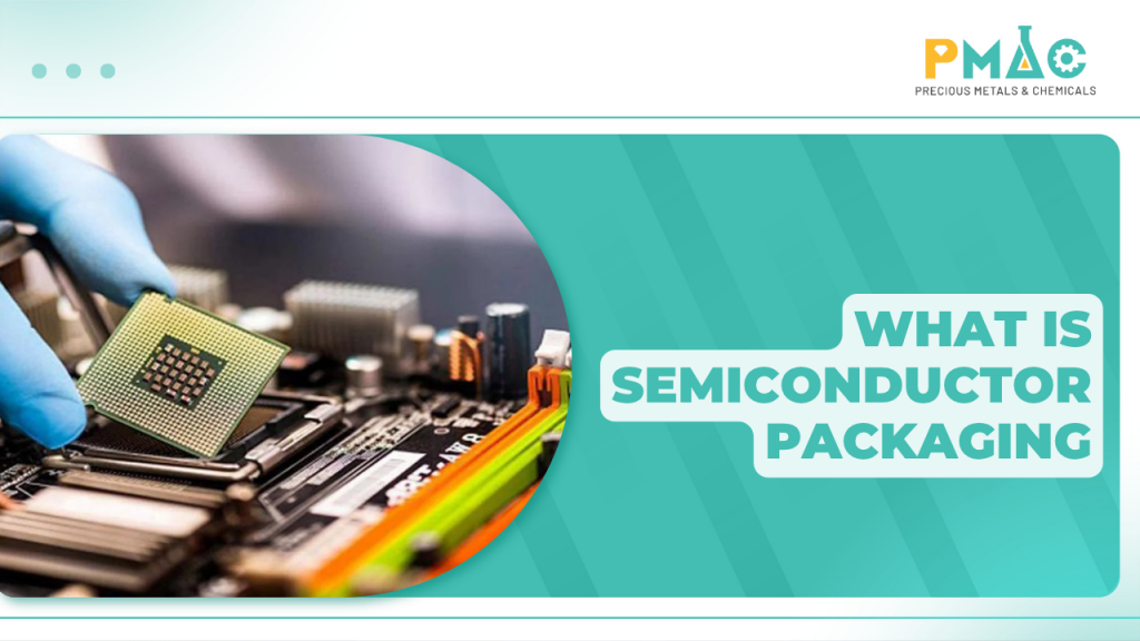
IV. What Are Semiconductor Assembly and Packaging?
Once wafer fabrication is complete, the wafer is diced into individual chips. However, these chips cannot yet be directly integrated into smartphones, computers, or other electronic devices. They must first be attached, interconnected, protected, and tested.
Intel describes this as the back end of semiconductor manufacturing—assembly and testing. One or more dies are mounted onto a package substrate, creating electrical connections, improving mechanical durability, and protecting the chip from environmental exposure.
Within this area, PMAC is expanding solutions related to die-attach materials, bonding wire, solder bumps, flux, die bonders, wafer dicing equipment, and probing systems.
As chip architectures become more complex, packaging is no longer simply an external protective layer. Advanced packaging technologies increasingly contribute directly to multi-chip interconnection, thermal management, and overall system performance. As a result, the relationship between packaging materials, equipment precision, and metrology capabilities is becoming increasingly important.
>> Learn more: Explore Semiconductor Packaging Solutions at PMAC
V. What Is the Role of Analysis and Metrology in Semiconductor Manufacturing?
In semiconductor manufacturing, quality control cannot wait until the chip is complete. Manufacturers need continuous visibility throughout the process: whether material composition is correct, film thickness meets requirements, surfaces are sufficiently flat, structures contain defects, or electrical resistance remains within specified limits.
As semiconductor structures become smaller, even a minor deviation in an early process step can affect multiple downstream stages. Analysis and metrology therefore become an integral part of process control rather than simply a final inspection step.
PMAC is developing this technology group with XRF, ICP-OES, ICP-MS, AAS, microscopy, SEM, AOI, X-Ray, film thickness measurement, surface profilometry, optical metrology, ellipsometry, and four-point probe systems.
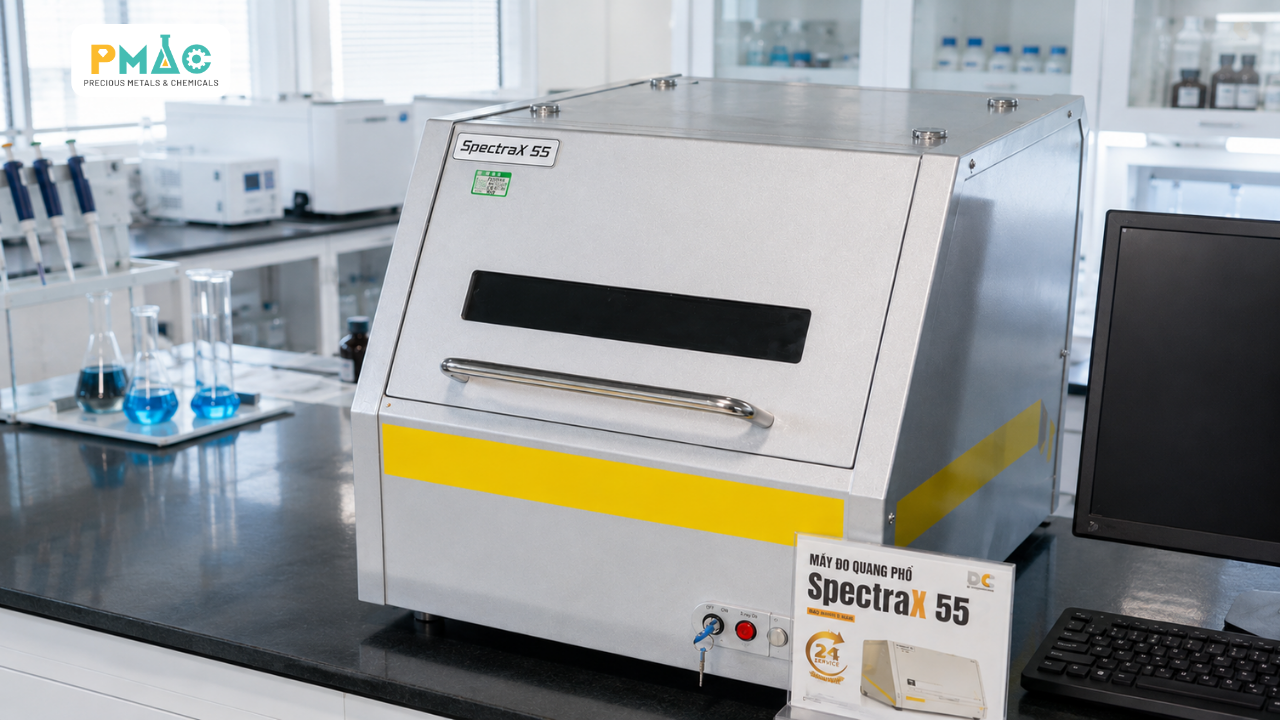
Figure 2: What Is the Role of Analysis and Metrology in Semiconductor Manufacturing?
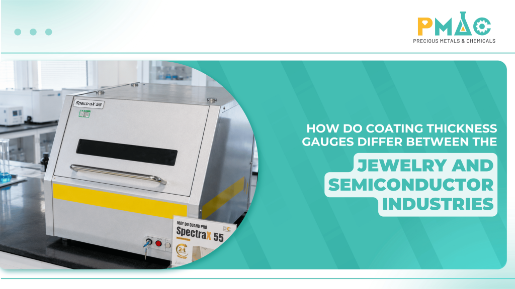
Each technology answers a different question. XRF can support elemental composition analysis or coating thickness measurement; ICP-OES and ICP-MS are used for elemental analysis at lower concentration levels; SEM enables detailed surface and structural observation; AOI and X-Ray help identify different types of defects; while four-point probe systems are used to evaluate the electrical properties of materials.
Data generated from these measurements helps manufacturers detect deviations earlier, identify root causes, and prevent issues from progressing further into the production line. This is also why semiconductor testing is increasingly interconnected with analysis, metrology, and process control capabilities.
>> Learn more: What Is Semiconductor Testing?
VI. What Does Semiconductor Factory Automation Include?
In semiconductor manufacturing, metrology is not limited to final-product inspection. Manufacturers need continuous information on whether material composition is correct, whether film thickness meets specifications, whether surfaces are sufficiently flat, whether structures contain defects, and whether electrical resistance remains within acceptable limits. As chip structures continue to shrink, even very small deviations can create larger problems in subsequent process steps.
For this reason, PMAC is expanding its analysis and metrology portfolio with XRF, ICP-OES, ICP-MS, AAS, SEM, microscopy, AOI, X-Ray, film thickness measurement, surface profilometry, optical metrology, ellipsometry, and four-point probe systems. Each technology provides different information about materials or processes, and this data allows manufacturers to identify deviations before they move further downstream.
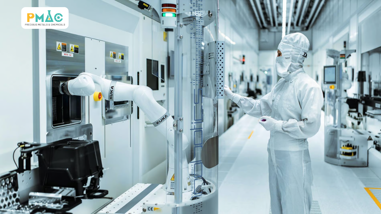
Figure 3: Semiconductor Factory Automation
VII. How Does PMAC Connect Technologies Across the Semiconductor Manufacturing Chain?
Looking across the entire process, semiconductor manufacturing can be seen as a sequence of interconnected capabilities: substrates provide the starting point; materials and chemicals create functional layers; equipment performs the required processing; assembly and packaging turn dies into usable devices; analysis and metrology control quality; and automation helps manufacturing stages operate more consistently. PMAC’s semiconductor portfolio is being developed around these same technology groups.
PMAC also does not intend to build its entire portfolio around a single supplier. Semiconductor manufacturing is a highly specialized industry in which different technology partners may have strengths in different parts of the process. PMAC therefore aims to connect an international technology partner network with the specific requirements of each customer, while also supporting the implementation of those technologies in real manufacturing environments.
VIII. How Is PMAC Developing Its Semiconductor Ecosystem?
Expanding into semiconductors does not mean PMAC is only now shifting from product sales to service delivery. An end-to-end service model has been developed over many years through PMAC’s experience in precious metals, electroplating, analysis and testing, and precious-metal recovery and refining. In semiconductors, this existing foundation is being extended into a more highly specialized technology ecosystem.
This becomes particularly important as Vietnamese companies seek to participate more deeply in the semiconductor supply chain, where expectations for quality, data, traceability, and technical support continue to rise.
>> Learn more: Why Are Vietnamese Companies Still Struggling to Enter the Semiconductor Supply Chain?
PMAC currently aims to support customers from technical consulting, application support, and technology selection through installation, commissioning, calibration support, maintenance, and training. The new element is therefore not the service model itself, but the broader range of technologies PMAC can connect across an increasingly comprehensive semiconductor manufacturing process.
From substrates and materials to equipment, packaging, and metrology, each technology creates value only when it is positioned correctly and operates effectively with the surrounding process steps. For PMAC, building a semiconductor ecosystem therefore goes beyond expanding a product portfolio. The focus is on connecting the right technologies, the right partners, and the right technical capabilities around the actual manufacturing needs of each customer.
Follow PMAC for more insights into semiconductor packaging, testing, and materials.
PMAC Joint Stock Company
Ho Chi Minh City Office:
4th Floor, HUTECH Building, D1 Road, Saigon Hi-Tech Park, Tang Nhon Phu Ward, Ho Chi Minh City, Vietnam
Hanoi Office:
22B O2, Linh Dam Peninsula, Hoang Liet Ward, Hanoi, Vietnam
Hotline: +84 387 235 878
Facebook: PMAC