

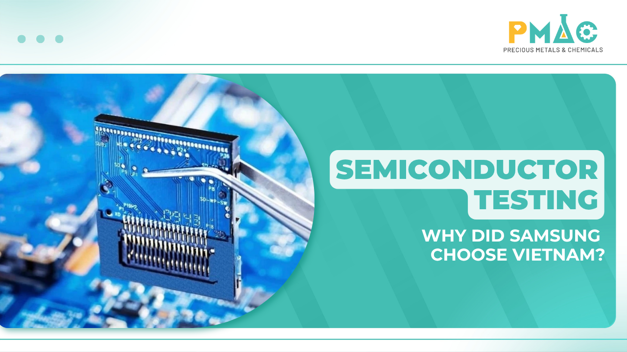
A semiconductor chip cannot be placed directly into a smartphone, computer, or automobile immediately after it is manufactured. Before shipment, manufacturers still need to confirm one critical point: does the chip actually function as designed? That is the role of semiconductor testing.
This concept has attracted greater attention in Vietnam after Reuters reported that Samsung Electronics plans to invest approximately VND 39 trillion, equivalent to US$1.5 billion, in a chip testing facility in Thai Nguyen. The plant is currently under construction and is expected to begin operations in November 2027. According to Reuters, this will be Samsung’s first semiconductor testing facility in Vietnam.
What is significant is not only the US$1.5 billion investment. Samsung has been manufacturing electronics in Vietnam for many years. The company’s decision to bring another stage of the semiconductor value chain to Thai Nguyen suggests that Vietnam has an opportunity to move beyond its role as an electronics manufacturing hub and participate in deeper stages of the chip industry.
So, what is semiconductor testing, why is it important, and what makes Vietnam an attractive choice for Samsung?
I. What Is Semiconductor Testing?
Semiconductor testing is the process of using specialized measurement equipment and test programs to determine whether a semiconductor device operates according to its design specifications. A chip may be extremely small, but it contains a highly complex electrical system. Variations in fabrication, materials, interconnections, or packaging can all cause a chip to operate incorrectly or inconsistently.
Testing systems therefore need to measure many parameters, including chip functionality, electrical signals, processing speed, power consumption, and performance under different operating conditions.
According to Advantest, ATE – Automated Test Equipment is used to determine whether semiconductor devices operate as designed. These systems are used at multiple stages of semiconductor manufacturing, from when the chips are still on the wafer to after they have been packaged into finished components.
Put simply, if fabrication creates the chip and packaging enables it to connect with a device, testing confirms that the chip can actually be used.
II. Are Chips Tested Before or After Packaging?
Semiconductor testing is not a single operation performed only at the end of the production line. One important testing stage takes place while individual dies are still on the wafer.
At this stage, the wafer is placed on a device called a wafer prober. A probe card with extremely small contact points connects each die to the tester. The system sends electrical signals and measures the response to identify dies that do not meet requirements. Detecting defective dies early is important because if a die already fails but still proceeds through dicing, packaging, and finishing, the manufacturer continues spending resources on a product that ultimately cannot be used.
Once qualified dies have been packaged, the chips proceed to final test. A test handler places individual devices into sockets connected to the tester. The equipment can test chips under different temperature conditions and then classify them according to the measured results. Advantest confirms that wafer testing is performed before packaging, while package or final testing takes place during the back-end stage.
Intel also describes assembly and test as the “second half” of semiconductor manufacturing. A silicon die leaving the fab still needs to be packaged, connected, and tested before it can be shipped to customers.
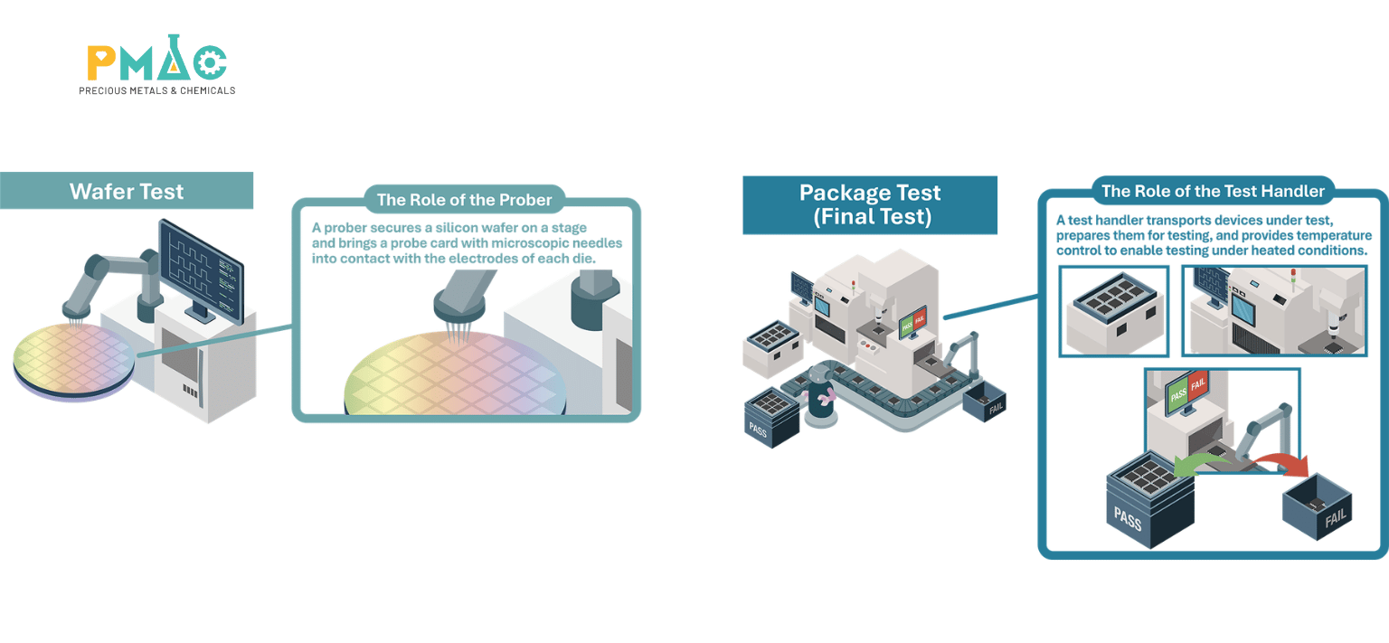
Figure 1: Semiconductor testing process
III. Why Is Semiconductor Testing So Important?
Testing may appear to be simply about finding defective chips and removing them. In reality, its value goes much further.
Data generated by test equipment allows manufacturers to identify where defects occur and whether they repeatedly appear in the same wafer area, production lot, or manufacturing process. This information can then be fed back to manufacturing and design teams to identify root causes and improve yield – the percentage of chips that meet specifications.
In large-scale semiconductor manufacturing, this has major economic implications. Even a small improvement in yield can increase the number of qualified products produced from the same number of wafers.
Testing must also balance competing priorities: more extensive testing increases the probability of detecting defects, but it also increases the time and cost per chip. An effective production line must therefore find the right balance between accuracy, speed, and cost.
This is why semiconductor test equipment is becoming increasingly sophisticated. For memory chips produced at very high volumes, modern systems can test multiple devices simultaneously to maintain throughput. Advantest notes that memory testers are specifically designed for high-volume manufacturing environments, where parallel testing capability is a key requirement.
IV. What Will Samsung Test in Vietnam?
According to the project documents reviewed by Reuters, the Thai Nguyen facility will be related to DRAM and NAND memory products. These two memory categories are widely used in smartphones, computers, servers, and many other electronic devices. DRAM mainly provides temporary memory that allows a system to process data while operating, while NAND is used for long-term data storage, such as in smartphones and SSDs.
What makes the project particularly notable is its timing, as the memory market is being reshaped by the AI boom. Growing demand for data center memory is forcing manufacturers to adjust production capacity, while demand for chips used in smartphones, computers, and conventional electronic devices remains substantial.
The new testing facility is therefore not an isolated project. It forms part of a broader effort to expand capacity across the global memory supply chain.
V. Why Is Samsung Continuing to Choose Vietnam?
Samsung has not published an official document listing every reason behind its decision to select Vietnam. It would therefore be inaccurate to claim that the decision was driven only by lower labor costs or investment incentives. However, when considering the project location, the existing industrial ecosystem, and Vietnam’s semiconductor development strategy, the choice of Thai Nguyen follows a clear logic.
First, Samsung is not starting from zero. The new facility is being built next to the company’s existing electronics manufacturing complex in Thai Nguyen. Samsung already has production infrastructure, a workforce, logistics capabilities, and a supplier network that have been developed over many years. Reuters reported that Samsung has invested more than US$23 billion in Vietnam, while more than 200 engineers and employees had already been deployed to the project site by April 2026.
For an industry that demands a high level of operational stability, an established ecosystem can significantly reduce complexity compared with building from scratch in a completely new location. Another important factor is that Vietnam already has a foundation in back-end semiconductor activities, including assembly, packaging, and testing after wafer fabrication.
Intel has operated an assembly and test facility in Vietnam for many years. Amkor and Hana Micron also have operations in the country. Reuters has therefore described Vietnam as an emerging semiconductor back-end hub.
In early 2026, FPT also announced an advanced semiconductor packaging and testing facility in Bac Ninh. It is the first facility of its kind owned and operated by a Vietnamese company, with functional test lines using ATE testers and handlers.
Samsung is therefore not entering a market that is completely unfamiliar with chip testing. Existing projects are gradually building the workforce, operational experience, and supporting service network needed for this sector.
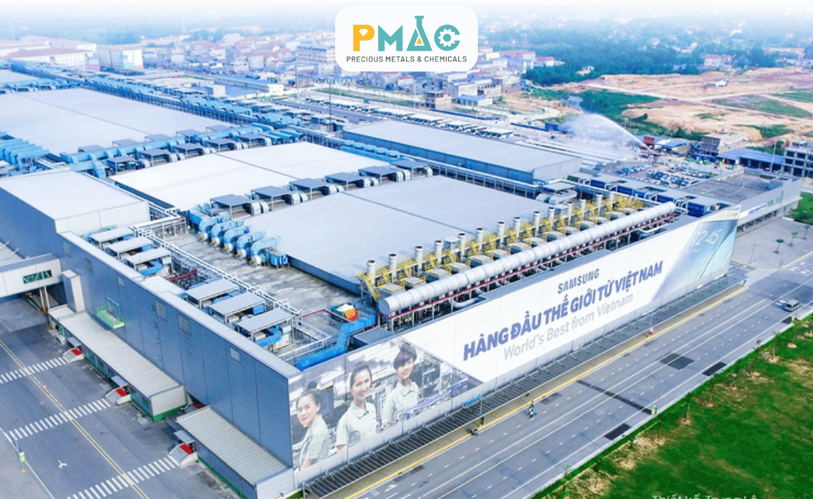
Figure 2: Samsung branch in Vietnam
VI. Vietnam Is Also Actively Investing in Packaging and Testing
Samsung’s investment direction is closely aligned with Vietnam’s semiconductor development strategy.
Under Decision 1018/QD-TTg, Vietnam aims to establish at least 100 chip design companies, one small-scale semiconductor fabrication plant, and 10 semiconductor packaging and testing facilities by 2030. Semiconductor industry revenue is targeted to exceed US$25 billion annually.
Notably, packaging and testing are identified as a separate development target. This reflects the reality that Vietnam does not necessarily need to begin its semiconductor ambitions by competing directly with the world’s most advanced fabs. In the near term, stages where Vietnam already has manufacturing experience and an FDI foundation offer a more practical entry point.
The workforce is also being developed in this direction. Vietnam’s semiconductor human resources development program targets at least 50,000 university-level semiconductor professionals by 2030, including around 35,000 working in areas beyond design, such as manufacturing, packaging, and testing.
However, this is also a significant challenge. Chip testing is not ordinary assembly work. Engineers must work with electronic circuits, measurement equipment, test programs, production data, failure analysis, and yield management. A facility may have advanced equipment, but without personnel capable of operating and optimizing the process, it will still struggle to create high-value output.
Figure 3: Semiconductor testing in Vietnam
VII. What Opportunities Could Samsung’s Testing Facility Create for Vietnam’s Ecosystem?
A semiconductor testing facility requires much more than a tester. An ATE system is surrounded by wafer probers, test handlers, probe cards, sockets, interface boards, temperature control systems, automation, data analysis tools, and many other supporting technologies. Operations also create demand for cleanrooms, maintenance, calibration, quality management, and technical materials.
This is where the project becomes particularly relevant for Vietnamese companies. The value of an FDI project is not measured only by the amount of capital invested or the number of direct jobs created. Greater value emerges when domestic companies can participate more deeply in the factory’s supply chain.
In semiconductor packaging, materials and surface treatment play an important role in creating stable electrical connections and ensuring component reliability. This also creates opportunities for companies supplying technical chemicals, electroplating materials, analytical equipment, and metal management solutions.
PMAC has explored these materials in greater detail in Semiconductor Plating Materials: New Opportunities for PMAC and Umicore. For production lines using gold, silver, palladium, or other valuable metals, monitoring and recovering these materials can also directly affect manufacturing costs. More information is available in PMAC’s article on Precious Metal Recovery Applications in Semiconductor Component Manufacturing.
Conclusion
Samsung’s planned US$1.5 billion investment reflects an important shift: Vietnam is gradually being selected not only for manufacturing finished electronic products, but also for a specific stage of the semiconductor value chain.
This does not mean Vietnam has already become a semiconductor powerhouse. Testing remains only one part of a very long value chain that extends from design and materials to wafer fabrication, packaging, and equipment manufacturing. The technology gap between these stages is also substantial.
However, for Vietnam, semiconductor testing represents a practical entry point. The country already has a large electronics manufacturing base, together with the presence of Intel, Amkor, Hana Micron, FPT, and now Samsung’s new project. At the same time, the Government has set clear targets for packaging, testing, and workforce development.
If Vietnam’s role in the supply chain remains limited to providing industrial space and labor, the value retained domestically will remain limited. But if local companies can gradually participate in materials, supporting equipment, process control, automation, maintenance, and technical services, each new facility can become another building block in a more mature domestic semiconductor ecosystem.
Semiconductor testing is therefore not only the process of confirming whether a chip works. For Vietnam, it could also become one of the most practical gateways to deeper participation in the global semiconductor value chain.
The expansion of packaging and testing activities is also creating new requirements for materials, technical chemicals, surface treatment, and quality control in semiconductor manufacturing.
PMAC Joint Stock Company
Ho Chi Minh City Office:
4th Floor, HUTECH Building, D1 Road, Saigon Hi-Tech Park, Tang Nhon Phu Ward, Ho Chi Minh City, Vietnam
Hanoi Office:
22B O2, Linh Dam Peninsula, Hoang Liet Ward, Hanoi, Vietnam
Hotline: +84 387 235 878
Facebook: PMAC