

A computer processor, an electric vehicle inverter, and a fast charger all rely on semiconductor devices, yet they are not necessarily built on the same material platform. Most processors and memory chips today still rely on Silicon, while SiC is increasingly used in high-voltage and high-power systems, and GaN is gaining attention in power supplies that require fast switching and high power density.
This distinction comes directly from the requirements of each application. A processor must integrate a very large number of transistors at a commercially viable manufacturing cost. An EV inverter, by contrast, must handle high current and voltage while minimizing power loss and heat generation. In chargers and data-center power supplies, switching speed can directly affect both system efficiency and overall size. A material that performs exceptionally well in one application may therefore offer little technical or economic advantage in another.
This is also why the development of semiconductor technology does not follow a simple path in which one new material successively replaces an older one. Silicon, SiC and GaN are likely to coexist, with each material being developed more aggressively in the application areas where its characteristics provide the greatest advantage. To understand why, it is first necessary to distinguish what these three materials are and how they are used in semiconductor devices.
I. What Are Silicon, SiC and GaN?
1. Silicon remains the most widely used platform in the semiconductor industry
Silicon – Si is the most widely used semiconductor element in the chip industry today. Silicon can be purified to extremely high levels, grown into single crystals and sliced into thin discs known as wafers. On the wafer surface, manufacturers successively form material layers and electronic structures that eventually become transistors and integrated circuits.
After decades of development, Silicon has become the foundation of an extensive manufacturing ecosystem. Processors, memory, microcontrollers, sensors and many other types of electronic circuits can all be fabricated on Silicon wafers.
Silicon’s most important advantage does not lie only in its intrinsic material properties. The semiconductor industry has developed the capability to manufacture large-diameter wafers, control defects effectively and process them at high volume with steadily improving cost efficiency. As a result, Silicon remains difficult to replace in applications where manufacturing scale, integration capability and cost are more important than extreme voltage or temperature performance.
2. SiC extends device capability in high-voltage and high-power environments
Silicon Carbide – SiC is a compound formed from Silicon and Carbon. Unlike Silicon, SiC belongs to the family of wide-bandgap semiconductors, meaning its material structure allows semiconductor devices to maintain their electrical properties under more demanding electrical and thermal conditions.
In practice, SiC is particularly important in power semiconductor applications. It can withstand much higher electric fields than Silicon and also offers strong thermal conductivity. These characteristics allow SiC devices to handle high voltage and power with lower losses in many applications.
This is why SiC is increasingly used in electric vehicle inverters, fast-charging infrastructure, solar energy systems, industrial electrical equipment and other high-voltage applications. However, SiC crystal and wafer manufacturing is more complex than Silicon processing, which means both material and manufacturing costs remain higher.
SiC is therefore not intended to replace Silicon in every type of chip. Its value becomes most apparent when voltage, power and thermal limitations become the primary constraints of a system.
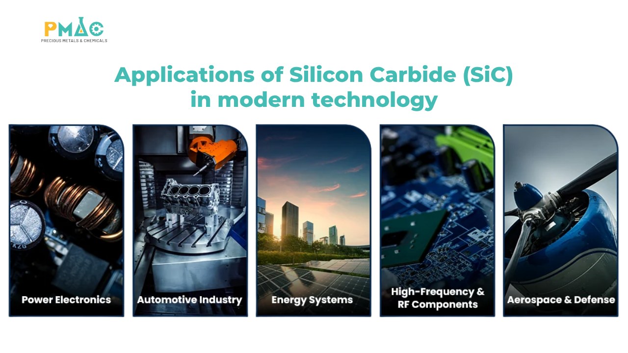
Figure 1. Typical applications of Silicon Carbide in power and industrial systems
3. GaN creates an advantage when switching speed becomes critical
Gallium Nitride – GaN is a compound of Gallium and Nitrogen and is also classified as a wide-bandgap semiconductor. While SiC is often associated with high voltage and strong thermal performance, GaN stands out in applications requiring fast switching and high-frequency operation.
This characteristic is particularly important in power-conversion circuits. Transistors in a power supply continuously switch on and off to convert voltage. When a transistor can transition between states faster while reducing switching losses, the system can operate at a higher frequency, which in turn allows certain passive components such as inductors and capacitors to become smaller.
This is one reason GaN is increasingly used in compact high-power chargers, data-center power supplies, industrial equipment and high-frequency systems.
One important distinction is that GaN is not always used in the same way as Silicon or SiC at the wafer level. In many commercial technologies today, manufacturers do not rely on a bulk GaN wafer. Instead, a GaN layer is grown on another substrate, such as Silicon or SiC. This gives rise to structures such as GaN-on-Si and GaN-on-SiC.
The underlying substrate is not merely a mechanical support. It can also affect thermal dissipation, crystal quality, wafer size and the manufacturing cost of the GaN device. For this reason, evaluating a semiconductor technology requires consideration of both the active semiconductor material and the substrate structure on which it is developed.
4. The three materials coexist across different application areas
| Material | Key advantages | Typical applications |
| Silicon | Mature technology, large wafers, strong cost efficiency and integration capability | Processors, memory, microcontrollers, sensors, electronic circuits |
| SiC | High-voltage capability, high-power handling, strong thermal conductivity | Electric vehicles, fast charging, energy systems, industrial applications |
| GaN | Fast switching, high-frequency operation, high power density | Chargers, data-center power supplies, RF, high-power-density power supplies |
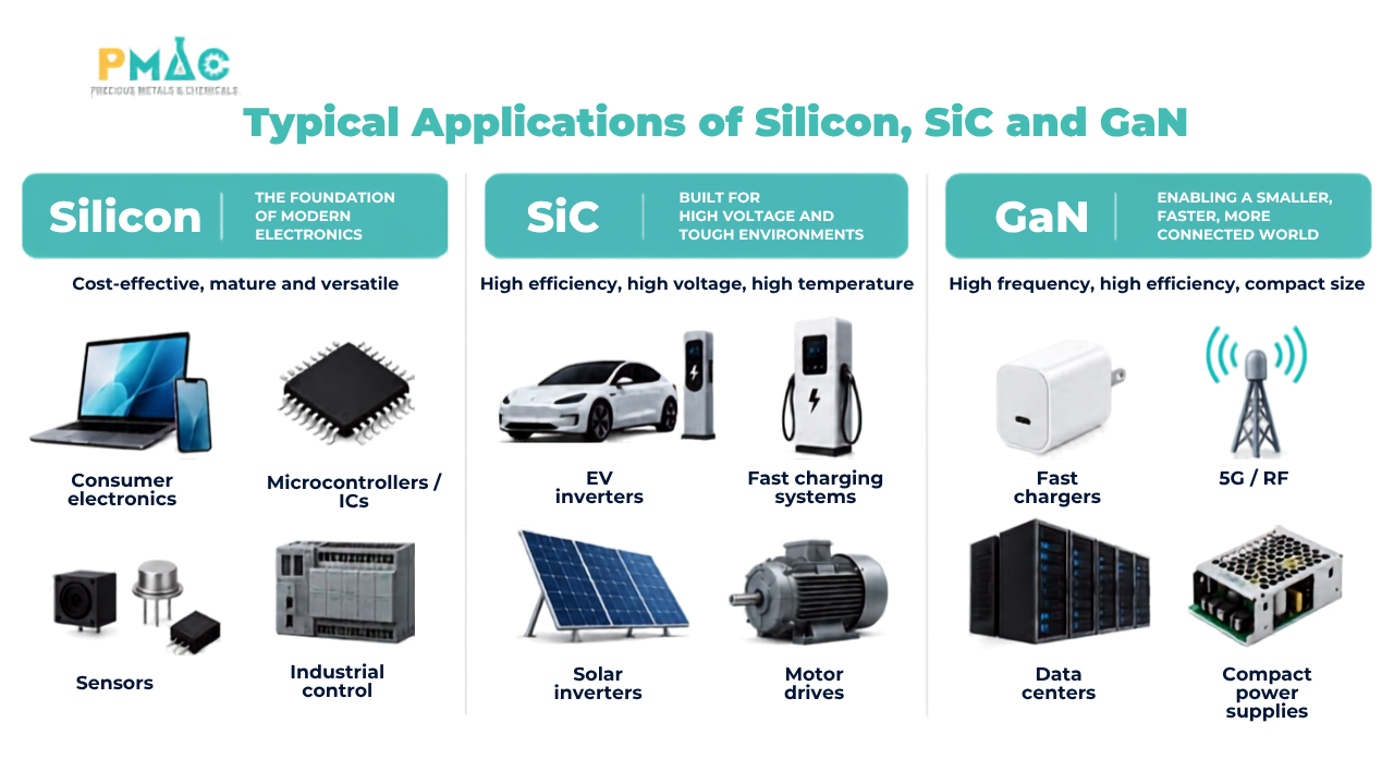
Figure 2. Silicon, SiC and GaN are suited to different application areas in semiconductor technology
II. Different Material Properties Create Different Operating Limits
Once Silicon, SiC and GaN have been defined, the next question is why simply changing the semiconductor material can make a device suitable for a processor, an electric vehicle or a fast charger in very different ways. The answer lies in the physical properties of each material, particularly bandgap, critical electric field and thermal conductivity.
Silicon has a bandgap of approximately 1.12 eV, while 4H-SiC is around 3.26 eV and GaN approximately 3.4 eV. Because SiC and GaN have significantly wider bandgaps, they are classified as wide-bandgap semiconductors. According to Infineon’s explanation of the bandgap properties of GaN and SiC, these characteristics allow the materials to withstand higher electric fields, operate under more demanding conditions and enable power-device designs that Silicon cannot achieve with the same efficiency.
| Typical property | Silicon – Si | 4H-SiC | GaN | Primary impact |
|---|---|---|---|---|
| Bandgap | ~1.12 eV | ~3.26 eV | ~3.4 eV | Ability to operate under demanding electrical and thermal conditions |
| Critical electric field | ~0.3 MV/cm | ~3 MV/cm | ~3–3.5 MV/cm | Voltage-blocking capability |
| Thermal conductivity | Moderate | Very high | Strongly dependent on structure and substrate | Ability to remove heat from the active region |
| Key strength | Scale, cost, integration capability | High voltage, high power | Fast switching, high frequency | — |
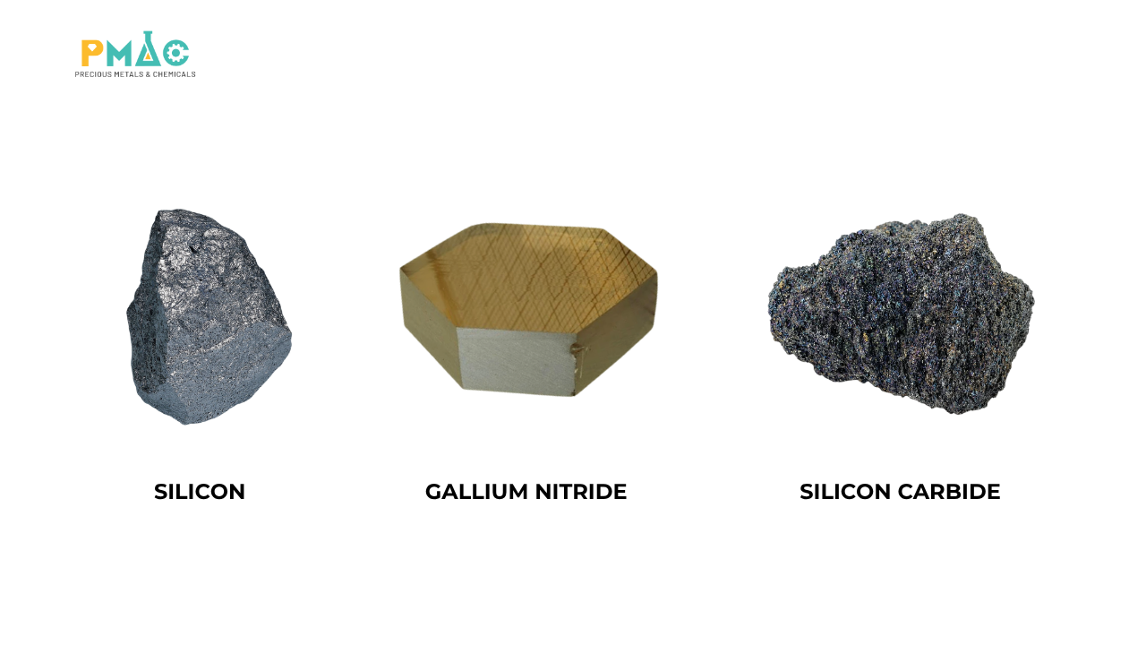
Figure 3. Silicon, Silicon Carbide and Gallium Nitride are three important material systems in semiconductor technology
III. Silicon Remains Dominant Because the Industry Has Optimized an Entire Ecosystem Around It
If the comparison were based only on physical properties, Silicon might appear less attractive than SiC and GaN. However, a semiconductor platform is not determined solely by material parameters. Manufacturing stability, wafer size, yield, equipment infrastructure and cost per chip are equally important.
Silicon has a major advantage in all of these areas. Over several decades, the semiconductor industry has built a complete ecosystem around Silicon wafers, covering crystal growth, thin-film deposition, lithography, doping, etching, metallization and testing. The 300 mm wafer platform is now well established in high-volume manufacturing, allowing manufacturers to process a large number of dies in each production cycle.
For this reason, switching from Silicon to SiC or GaN does not automatically create an advantage for CPUs, GPUs, memory, microcontrollers or many other integrated circuits. These products require high transistor density, extremely mature processes and commercially viable manufacturing costs more than they require extreme voltage capability.
Silicon itself has also not reached the end of its optimization potential. Manufacturers continue to reduce wafer thickness, optimize transistor structures and improve the performance of Silicon power devices. This shows that the development of SiC and GaN is not simply a story of “new materials replacing old materials.” Instead, the industry adopts alternative materials when Silicon is no longer the most efficient option for a specific requirement.
IV. SiC Becomes Particularly Valuable When Voltage and Power Are the Main Constraints
The advantages of SiC are most evident in power semiconductor devices. A power transistor must perform two opposing functions: when switched on, it should conduct current with minimal loss; when switched off, it must block high voltage without breaking down.
With Silicon, increasing the voltage-blocking capability generally requires a thicker region of semiconductor material. As this region becomes thicker, electrical resistance increases, which results in more energy being converted into heat. As system voltage and power continue to rise, this trade-off becomes increasingly difficult to manage.
SiC has a critical electric field approximately one order of magnitude higher than Silicon. As a result, a SiC device can withstand a comparable voltage using a thinner structure, thereby reducing resistance and associated losses. SiC also offers very strong thermal conductivity, providing another advantage when devices must handle high power density.
This is why SiC is increasingly associated with electric vehicles, inverters, fast-charging infrastructure, renewable energy and industrial electrical equipment. Reducing losses in a power device does more than improve the transistor itself. It can also reduce the amount of heat that must be managed, decrease part of the cooling requirement and improve overall system efficiency.
The development of SiC is also reflected in increasing wafer sizes. Major manufacturers are transitioning from 150 mm to 200 mm wafers to increase the number of dies per wafer and progressively improve the economics of SiC manufacturing. This transition is significant because physical advantages only become commercial advantages when a material can be manufactured consistently and at sufficient volume.
V. GaN Creates a Different Advantage: Faster Switching Can Reduce Overall System Size
While SiC stands out in high-voltage and high-power applications, GaN becomes particularly attractive when the challenge shifts toward switching speed.
In a power supply, a transistor does not simply turn on once and remain in that state. It continuously switches on and off to convert voltage. Each transition generates some energy loss. If the transistor can switch faster while losing less energy during each cycle, the system can operate at a higher frequency.
This is where GaN provides a significant advantage. According to Infineon’s overview of GaN semiconductor properties, its wide bandgap and electron-transport characteristics make GaN suitable for devices requiring fast switching, low losses and high power density.
The benefit extends beyond the transistor itself. When switching frequency increases, certain passive components in the power supply, such as inductors and capacitors, can also be made smaller. Therefore, when a GaN charger is smaller, the explanation is not simply that “the GaN chip is smaller than a Silicon chip.” Rather, GaN allows the entire power system to be redesigned around a higher switching frequency.
This is why GaN is increasingly used in high-power chargers, data-center power supplies and equipment where high power density must be achieved within limited physical space.
VI. SiC and GaN Solve Different Problems Rather Than Competing for a Single Winner
When SiC and GaN are compared directly, it is easy to ask which one is better. Without defining the application, however, that question has little meaning.
SiC generally offers clearer advantages when a system must handle high voltage, high power and substantial thermal loads. GaN performs particularly well when the main requirements involve switching speed, frequency and system miniaturization. These operating regions can overlap, meaning manufacturers may consider both technologies in certain applications depending on efficiency, voltage, circuit architecture, cost and supply-chain maturity.
A simple way to understand the distinction is:
- Silicon is well suited when the priorities are scale, cost and integration capability.
- SiC is well suited when the limitations to overcome involve voltage, power and heat.
- GaN is well suited when the limitations involve switching speed and power density.
The industry is therefore not evolving along a linear path of Silicon → SiC → GaN. Instead, all three platforms are coexisting and becoming increasingly specialized for different application regions.
VII. With GaN, the Underlying Substrate Also Influences Performance and Cost
GaN also illustrates a more complex aspect of semiconductor technology: the material used to form the transistor and the material used as the substrate are not always the same.
In many commercial devices, the GaN layer is grown on another wafer. Two common structures are GaN-on-Si and GaN-on-SiC.
GaN-on-Si takes advantage of Silicon’s major strengths in wafer size and manufacturing infrastructure. If GaN can be grown reliably on large Silicon wafers, manufacturers have an opportunity to leverage part of the existing production infrastructure and reduce cost per die.
However, GaN and Silicon have different crystal structures and thermal-expansion behavior. When the GaN layer is grown at high temperature and subsequently cooled, these differences can generate mechanical stress, wafer bowing or crystalline defects. This is why buffer layers and epitaxial-process control are critical in GaN-on-Si technology.
GaN-on-SiC, in contrast, provides better thermal performance and stronger material compatibility, making it attractive for applications requiring very high power and frequency. However, SiC substrates are more expensive than Silicon, which changes the economic equation.
Therefore, even when the active material remains GaN, simply changing the underlying substrate requires manufacturers to reconsider crystal defects, thermal management, wafer size and cost. This demonstrates clearly that the substrate is not merely a supporting platform beneath the device.
VIII. Strong Material Properties Must Still Overcome the Challenges of Wafer Quality, Defects and Yield
Suppose a material has an extremely high critical electric field, but its wafers are difficult to manufacture, contain many defects or exhibit poor epitaxial uniformity. In that case, fewer dies on each wafer will meet specifications, increasing the cost of every usable chip. This is why yield – the proportion of devices that meet requirements – is just as important as the material’s physical properties.
Wafer size also has a direct impact on manufacturing efficiency. Larger wafers allow more dies to be processed within a single production cycle, but they also make control of flatness, temperature, stress and layer uniformity increasingly difficult.
Silicon has already reached a highly mature 300 mm manufacturing platform. SiC is moving strongly toward 200 mm, while GaN-on-Si is also progressing toward 300 mm. These dimensions reflect different levels of manufacturing maturity rather than merely the physical size of the wafer.
A semiconductor material therefore has to move through the entire chain:
material properties → wafer quality → epitaxy → fabrication process → defects → yield → cost per good die
before its theoretical advantages can become practical commercial value.
IX. Materials, Equipment and Metrology Must Be Considered Within the Same Semiconductor Manufacturing Process
After the wafer and epitaxial layers have been formed, the semiconductor device still has to pass through multiple processes including thin-film deposition, lithography, etching, thermal processing, metallization and measurement. Changing the underlying material therefore often requires adjustments across the downstream process as well.
This is also why PMAC does not build its semiconductor portfolio around a single wafer category. PMAC’s current technology portfolio spans Silicon, SOI, SiC and GaN, along with thin-film materials, CVD/ALD precursors, metallization materials, wafer-processing equipment and analytical and metrology solutions.
At a broader level, the PMAC industrial ecosystem is also being developed to connect materials, equipment, analysis and metrology, and technical support around specific manufacturing requirements rather than treating them as isolated product categories.
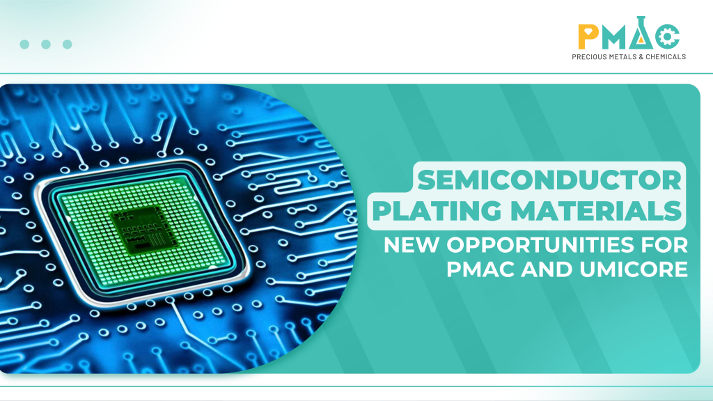
This relationship becomes particularly important in metallization. A metal layer may be extremely thin, but its quality can directly influence electrical conductivity, contact reliability and device stability. PMAC has discussed the relationship between materials and process conditions in greater detail in Semiconductor Plating Materials: New Opportunities for PMAC and Umicore.
From this perspective, choosing Si, SiC or GaN is only the starting point. The final value depends on whether downstream processes can be controlled consistently enough to translate the material’s advantages into actual device performance.
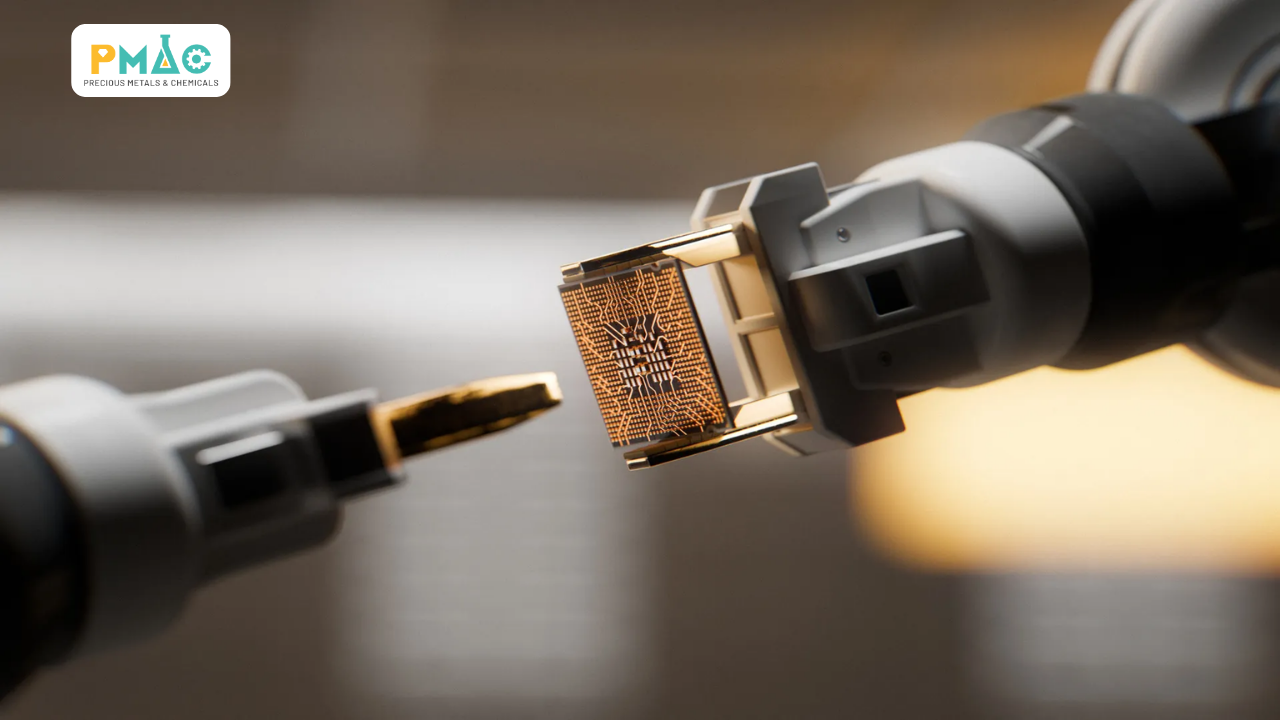
Figure 4. Analysis, metrology and process control are critical links in semiconductor manufacturing
X. Semiconductor Technology Is Moving from One Dominant Material Toward a Multi-Material Ecosystem
The development of SiC and GaN does not mean that Silicon is about to disappear. What is happening instead is that the semiconductor industry is increasingly selecting the right material for the right function.
Silicon continues to play a central role in processors, memory and most integrated circuits requiring high levels of integration. SiC expands the design space for high-voltage and high-power systems. GaN enables higher switching frequencies and greater power density in power-system designs.
All three platforms can even coexist within the same system. An AI data center, for example, may use Silicon for processing devices while relying on GaN or SiC in the power infrastructure to convert electrical energy more efficiently.
This is also why the semiconductor supply chain extends far beyond chip design and fabrication. Opportunities also exist in wafers, epitaxial materials, high-purity chemicals, metallization, manufacturing equipment, analysis and metrology – the capabilities that determine whether a material can successfully move from research into high-volume manufacturing.
Silicon, SiC and GaN are therefore not competing in a race to determine one universally superior material. Each platform expands a different operating boundary of semiconductor technology, and the final choice must always depend on the requirements of the application, manufacturing capability and overall system efficiency.
PMAC Joint Stock Company
Ho Chi Minh City Office:
4th Floor, HUTECH Building, D1 Road, Saigon Hi-Tech Park, Tang Nhon Phu Ward, Ho Chi Minh City, Vietnam
Hanoi Office:
22B O2, Linh Dam Peninsula, Hoang Liet Ward, Hanoi, Vietnam
Hotline: +84 387 235 878
Facebook: PMAC