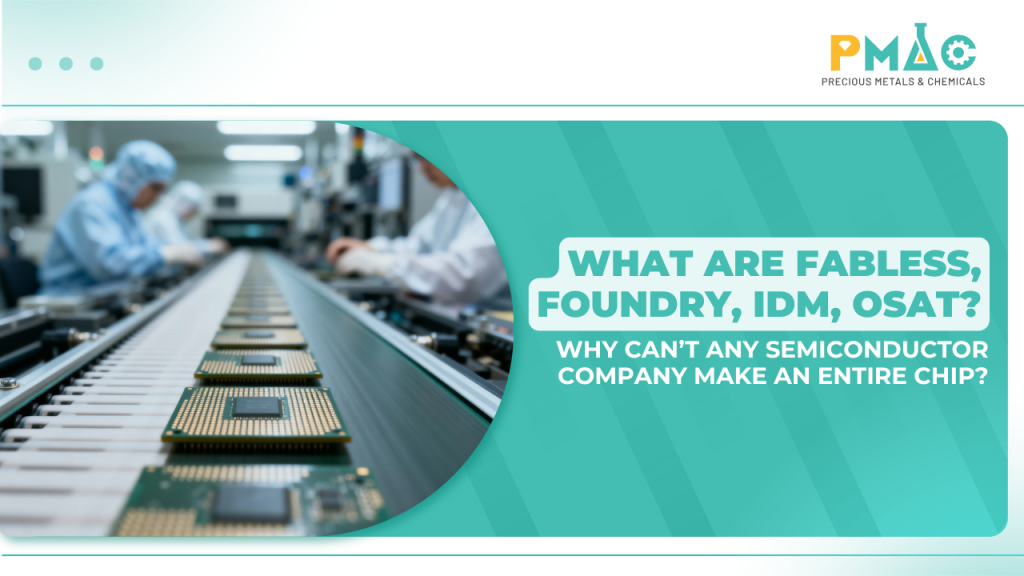


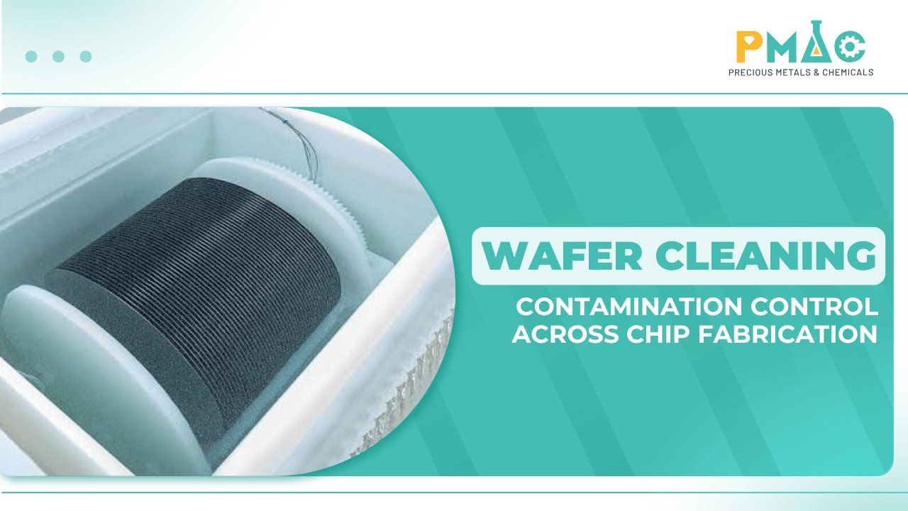
Wafer cleaning helps control particles, chemical residues, and metal contaminants during chip fabrication. Explore methods, equipment, and quality checks.
A semiconductor wafer undergoes numerous processing steps before it becomes part of a finished chip. Thin-film deposition, photolithography, etching, and chemical mechanical polishing (CMP) each modify the wafer surface, often leaving behind microscopic particles, chemical residues, or unwanted metallic impurities. Although these contaminants may be invisible to the naked eye, they can interfere with subsequent processes and compromise device quality.
This is why wafer cleaning is not a one-time preparation step. It is a recurring part of semiconductor manufacturing, helping maintain surface cleanliness, protect delicate structures, and reduce the risk of defects as fabrication progresses.
I. What Is Wafer Cleaning?
Wafer cleaning is the process of removing unwanted materials from a semiconductor wafer surface to prepare it for subsequent fabrication steps. Its purpose is not simply to make a wafer visibly clean, but to achieve the surface conditions required for a specific manufacturing process.
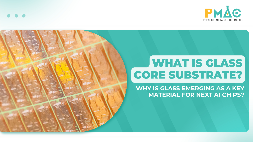
A wafer is a thin semiconductor substrate, typically made of silicon, on which electronic structures are built to create integrated circuits. During fabrication, successive material layers are deposited, patterned, modified, and selectively removed. These repeated processes continually change the wafer surface and create opportunities for contamination, even in highly controlled cleanroom environments.
According to semiconductor equipment manufacturers such as Lam Research and Tokyo Electron, cleaning is performed repeatedly between fabrication steps to remove unwanted particles and residues while preparing the wafer for further processing.
However, cleaning requirements vary considerably depending on the wafer’s condition. A bare silicon wafer may tolerate treatments that would be unsuitable for a patterned wafer containing metal interconnects, dielectric layers, or fragile microscopic structures.
Effective wafer cleaning must therefore achieve two objectives simultaneously: removing unwanted contamination and preserving the materials and structures that need to remain intact.
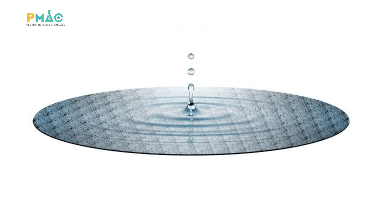
Hình 1. Wafer surface preparation and cleaning help maintain the conditions required for semiconductor fabrication.
II. Common Types of Wafer Contamination and Their Effects
Surface cleanliness plays a critical role in determining how accurately new materials and circuit structures can be formed. As semiconductor features become smaller and more complex, the tolerance for contamination becomes increasingly demanding. A particle or residue that is insignificant in one process may cause serious defects in another.
Wafer contamination can originate from the manufacturing environment, processing equipment, chemicals, handling operations, or materials used during fabrication. Understanding the type and source of contamination is essential because different contaminants require different cleaning approaches.
1. Particles and Microscopic Debris
Particles can be introduced through the cleanroom environment, process equipment, wafer handling, transportation, or previous manufacturing steps. Once deposited on a wafer surface, they may interfere with thin-film formation or disrupt the patterning of extremely small circuit features.
The impact depends on the particle’s size, location, and the requirements of the process being performed. A particle that causes no measurable issue during one operation may become a critical defect during a later step with tighter surface-quality requirements.
For this reason, particle contamination control requires more than simply removing visible debris. Manufacturers must evaluate whether the remaining particles fall within the limits established for the next fabrication stage.
2. Organic Residues and Residual Chemicals
Photolithography involves coating a wafer with photoresist, a light-sensitive material used to define circuit patterns. Once the patterned material has served its purpose, the remaining photoresist generally needs to be removed.
However, stripping and other processing steps may leave behind organic residues, polymers, or chemical by-products. If these materials remain on the surface, they can interfere with subsequent treatment or affect the adhesion of newly deposited layers.
This makes post-lithography cleaning an important part of process integration. Removing photoresist is not necessarily the final step; the wafer may also require additional cleaning to achieve the surface condition needed for the next operation.
3. Metallic Contamination
Unwanted metal contaminants may originate from process chemicals, water, equipment components, or previous fabrication steps. In sensitive semiconductor structures, even low concentrations of certain metallic impurities can affect electrical characteristics and device reliability.
Controlling metallic contamination therefore involves more than wafer cleaning alone. Chemical purity, equipment condition, process control, and suitable analytical methods all contribute to preventing unwanted metals from reaching the wafer surface.
This is also why material specifications matter when selecting chemicals for semiconductor manufacturing. A chemical that performs its primary function effectively may still be unsuitable if its impurity profile does not meet the requirements of the application.
4. Native Oxides and Post-Process Residues
Silicon surfaces can form a thin native oxide layer when exposed to the surrounding environment. Depending on the fabrication step, this oxide may need to be removed before further processing.
Residual cleaning chemicals or rinse water can also leave unwanted deposits or introduce contamination during drying. These issues may affect surface quality even after the primary cleaning process has removed the original contaminants.
However, not every oxide layer should be removed. Many semiconductor processes intentionally create oxide layers for insulation, protection, or other functions. The cleaning method must therefore distinguish between unwanted surface materials and functional layers that need to be preserved.
| Contaminant Type | Potential Sources | Possible Effects |
| Particles | Environment, equipment, wafer handling | Surface defects, interference with thin-film deposition |
| Organic residues | Photoresist, solvents, chemical reactions | Poor surface preparation, interference with film adhesion |
| Metallic impurities | Chemicals, process water, equipment | Changes in electrical properties and device reliability |
| Unwanted oxides | Surface reactions and environmental exposure | Interference with certain subsequent fabrication steps |
| Rinsing residues | Cleaning solutions and drying operations | Surface stains, deposits, or recontamination |
The key principle is that wafer cleaning is not about removing everything from the surface. It is about selectively eliminating contaminants that could compromise the next manufacturing step.
This distinction provides the foundation for choosing suitable cleaning chemicals, equipment, and process conditions.
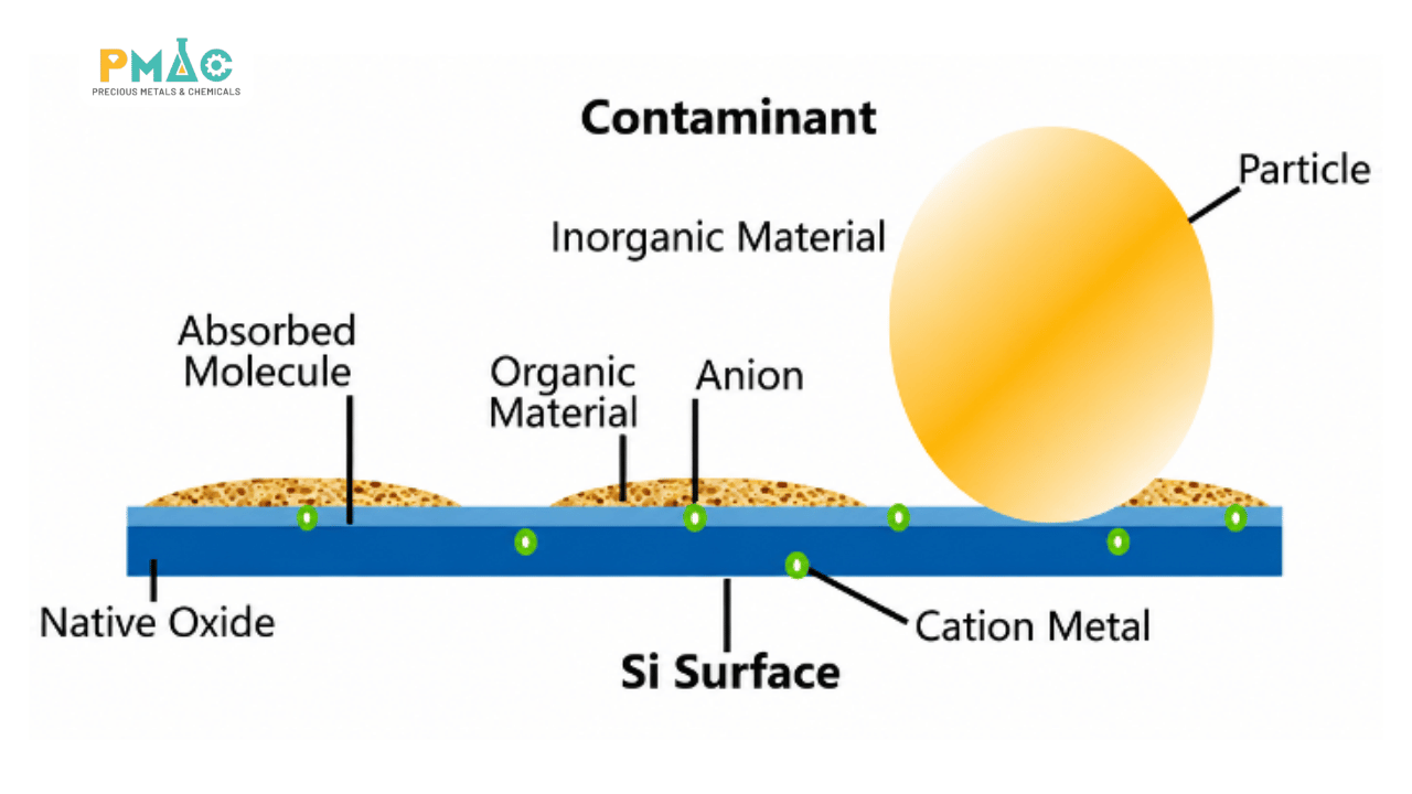
Figure 2. Common wafer contaminants and unwanted surface oxides.
III. Where Does Wafer Cleaning Fit into Semiconductor Manufacturing?
It is easy to assume that wafers only need to be cleaned before entering a fabrication line. In practice, semiconductor manufacturing involves repeated cycles of deposition, patterning, etching, material removal, and surface treatment. Each stage can introduce new residues or change the condition of the wafer surface.
As a result, cleaning operations are integrated at multiple points throughout the fabrication process, with different objectives depending on the preceding and subsequent steps.
Before Thin-Film Deposition
Before a new material layer is deposited, the wafer surface must meet the conditions required by the selected deposition process. Particles and unwanted residues can affect film formation, uniformity, and other critical properties.
Surface preparation is particularly important for processes that demand precise control of material thickness and interfaces. Technologies such as PVD, CVD, and ALD have different deposition mechanisms, but all require appropriate surface conditions for the intended application.
PMAC discusses these technologies in greater detail in How Are PVD, CVD, and ALD Different?.
Before Certain Photolithography Steps
Surface contamination can affect photoresist coating and the quality of the patterns formed during photolithography. Particles, chemical residues, and unsuitable surface conditions may interfere with the uniformity or adhesion of the photoresist layer.
Preparing the wafer surface therefore helps establish suitable conditions for pattern formation and subsequent processing.
After Etching and Photoresist Removal
Etching and photoresist stripping can leave reaction by-products, polymers, and other residues on the wafer. These materials may need to be removed before the next fabrication step to prevent contamination from carrying forward.
The appropriate cleaning method depends on the materials exposed after etching and the chemical or physical characteristics of the residues.
After Chemical Mechanical Polishing (CMP)
Chemical mechanical polishing combines chemical reactions and mechanical action to achieve a flatter wafer surface. However, the process may leave abrasive particles, slurry residues, and removed material on the wafer.
Post-CMP cleaning must remove these contaminants while protecting the surface and structures created during earlier fabrication steps.
The chemicals, equipment, process duration, and quality-control requirements therefore vary according to where cleaning takes place in the manufacturing flow.
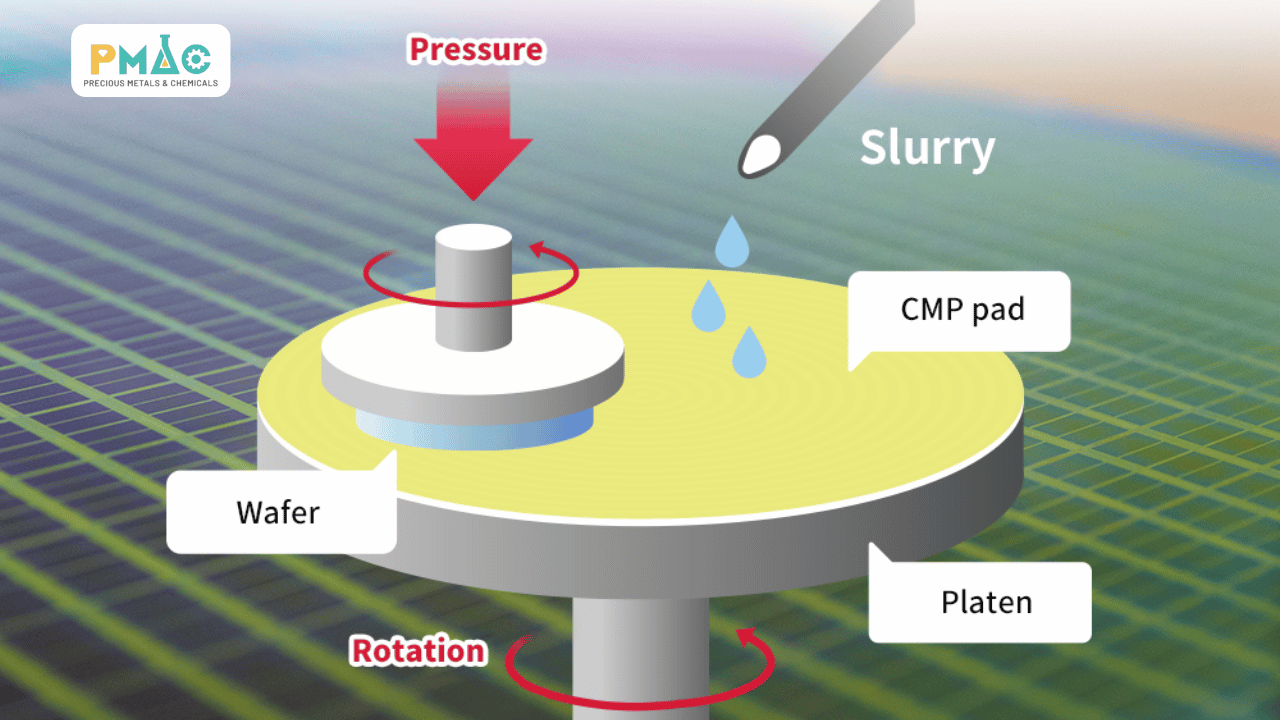
Figure 3. Chemical mechanical polishing combines mechanical action and slurry chemistry
Rather than functioning as a single standalone operation, wafer cleaning supports the continuity and reliability of multiple interconnected fabrication processes.
IV. Wafer Cleaning Methods Used in Semiconductor Manufacturing
No single cleaning method can effectively remove every type of contaminant from every semiconductor surface. Manufacturers use different approaches involving liquid chemicals, gases, plasma, and controlled physical forces, often followed by carefully managed rinsing and drying.
The choice depends not only on cleaning effectiveness but also on material compatibility, surface protection, process requirements, and equipment integration.
1. Wet Chemical Cleaning
Wet cleaning uses chemical solutions, solvents, or high-purity water to remove unwanted materials from a wafer surface.
One well-established approach is RCA cleaning, which was originally developed for silicon wafer preparation. Its standard cleaning sequence generally includes treatments designed to address particles, organic contamination, and metallic impurities.
For example, SC-1 is commonly associated with particle and organic residue removal, while SC-2 is used primarily to address metallic contamination. Variations of these processes may be combined with oxide treatment, rinsing, and drying when appropriate.
However, a cleaning chemistry suitable for bare silicon may not be compatible with a wafer containing exposed metal layers or sensitive structures. The selection process must consider both contaminant removal and the potential effects on materials that should remain unchanged.
Chemical purity is another critical factor. Cleaning agents, process water, and handling systems must be controlled to avoid introducing additional contaminants during treatment.
Manufacturers such as RENA offer different wet-processing solutions for semiconductor cleaning applications, illustrating why process chemistry and equipment design must be considered together.
2. Dry Cleaning and Plasma-Based Treatment
Some cleaning methods use gases or plasma to remove unwanted materials without immersing the wafer in liquid chemicals.
Oxygen plasma, for example, can be used in suitable applications to remove organic residues or remaining photoresist. Such processes are particularly relevant when the material to be removed can be treated effectively through plasma-based reactions.
Dry cleaning offers specific advantages for certain applications, but it is not a universal replacement for wet cleaning. Its suitability depends on the contaminant, exposed materials, surface condition, and operating requirements.
The decision should therefore be based on the technical objective rather than the assumption that a process without liquid chemicals is automatically preferable.
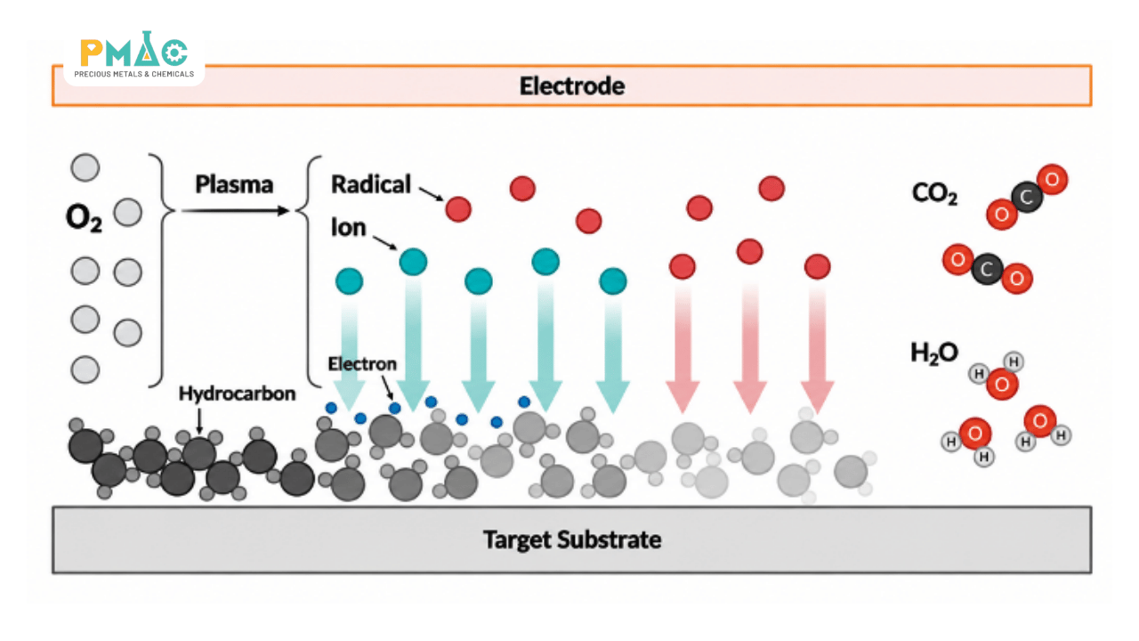
Figure 4. Reactive species generated by oxygen plasma help break down and remove organic residues from surfaces
3. Physically Assisted Cleaning
Some cleaning systems use controlled liquid flow, gas flow, acoustic energy, or other physical mechanisms to help dislodge particles from the wafer surface.
These techniques may complement chemical cleaning by improving particle removal under suitable conditions. However, greater cleaning force does not necessarily mean better results.
For wafers containing small or fragile structures, excessive mechanical or fluid forces can damage the surface or deform patterned features. Cleaning effectiveness must therefore be balanced against the risk of structural damage.
4. Rinsing and Drying
After contaminants have been removed, wafers generally undergo rinsing and drying to reduce residual chemicals, water, and surface deposits.
These operations are not merely finishing steps. Poorly controlled rinsing or drying can cause stains, leave residues, introduce new contamination, or damage delicate structures.
According to Tokyo Electron, drying technology is an essential part of wafer cleaning. This becomes particularly important as semiconductor devices incorporate increasingly complex and fragile features.
An effective cleaning process must therefore be evaluated as a complete sequence, from contaminant removal through rinsing, drying, and transfer to the next fabrication step.
V. Key Considerations When Selecting a Wafer Cleaning Solution
For companies developing or upgrading semiconductor manufacturing capabilities, equipment selection should not begin with price comparisons or the latest advertised cleaning technology.
The starting point should be a clear understanding of the wafer’s current condition, the contaminants that need to be removed, and the surface requirements of the next process step.
From there, manufacturers can evaluate the technical and operational factors that determine whether a cleaning solution is suitable.
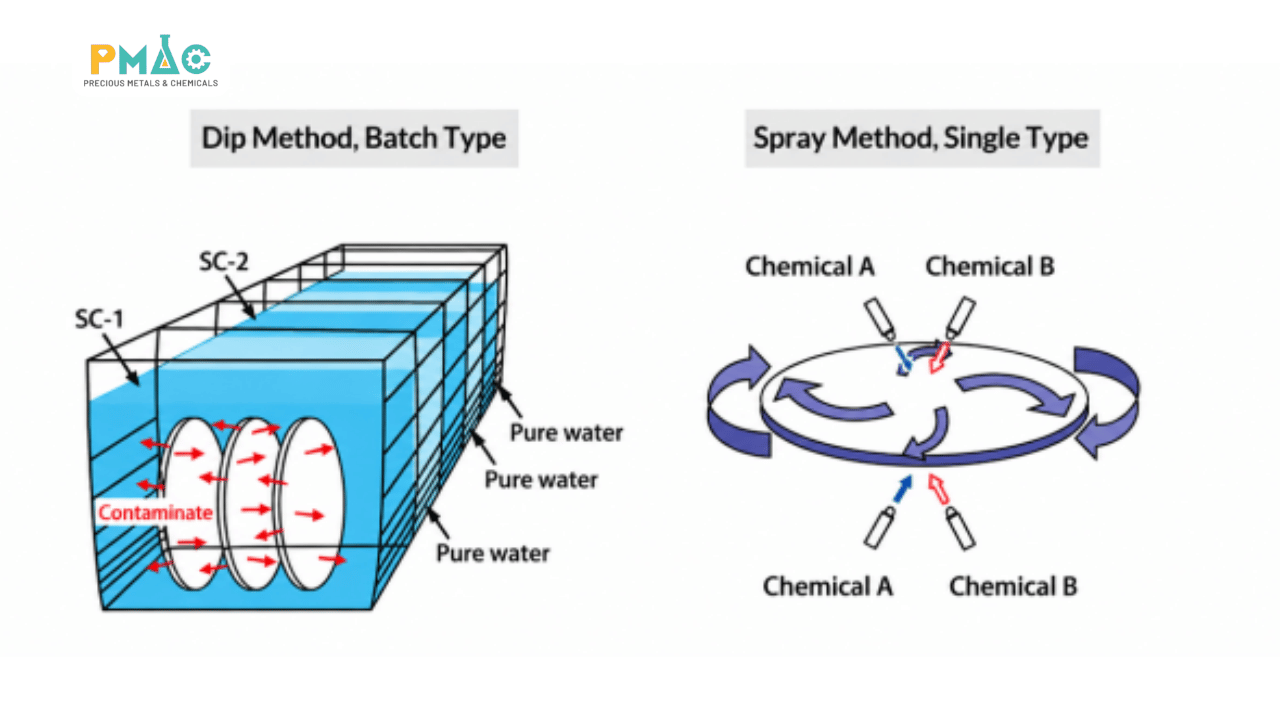
Figure 5. Batch immersion and single-wafer spray cleaning use different approaches to wafer treatment and process control
1. Vật liệu và trạn
1. Wafer Materials and Surface Conditions
Bare silicon wafers, wafers with oxide layers, and wafers containing multiple metal structures may require significantly different cleaning approaches.
A chemical that removes contaminants effectively but damages a functional layer cannot be considered suitable for the application. Manufacturers must identify which materials are present, which substances need to be removed, and which structures must remain intact.
This information is essential before selecting process chemicals or establishing operating conditions.
2. Types of Contamination
Particles, organic residues, and trace metals behave differently and may require different removal mechanisms.
Identifying the contamination source helps engineers choose appropriate treatments and avoid unnecessary processing steps. Without this information, increasing chemical concentrations or extending cleaning time may add cost without resolving the underlying problem.
It can also increase the risk of unwanted changes to the wafer surface.
3. Surface Protection Requirements
Cleaning performance must be assessed alongside its effects on the underlying materials and fabricated structures.
This is particularly important when wafers contain delicate features or multiple functional layers. An aggressive process may remove contaminants successfully while causing unacceptable material loss or surface damage.
For this reason, manufacturers should evaluate surface condition after cleaning rather than relying solely on contaminant-removal performance.
4. Throughput and Process Integration
In an industrial production environment, a cleaning system must support both surface-quality requirements and manufacturing throughput.
Important factors include wafer processing capacity, cycle time, consistency between production lots, equipment configuration, and integration with existing manufacturing systems.
One major decision is whether to use batch cleaning or single-wafer cleaning.
| Evaluation Criteria | Batch Cleaning | Single-Wafer Cleaning |
| Processing approach | Multiple wafers processed in one cycle | Individual wafers processed separately |
| Key control requirements | Uniformity across wafers and management of shared process chemistry | Precise process control and repeatability for each wafer |
| Operational considerations | Batch size, chemical consumption, cycle time | Processing time per wafer, equipment configuration |
| Typical suitability | Processes that allow multiple wafers to be treated together | Applications requiring more individualized process control |
Neither approach is inherently superior in every situation. The appropriate configuration depends on wafer characteristics, cleaning requirements, production capacity, and the broader process flow.
5. Long-Term Operating Costs
Equipment purchase price is only one component of the total cost of a wafer cleaning system.
Manufacturers must also consider chemical consumption, ultrapure water requirements, energy use, consumables, maintenance, and wastewater treatment. A system with a lower initial price may not provide the best long-term value if operating costs are high or cleaning performance is inconsistent.
Equipment specifications and supplier documentation provide a useful starting point, but actual performance should be evaluated against the intended manufacturing conditions.
A sound investment decision must balance cleaning quality, production throughput, process reliability, and total operating cost.
VI. How Can Manufacturers Verify Wafer Cleaning Performance?
A wafer that appears clean to the naked eye is not necessarily suitable for semiconductor fabrication. Cleaning performance must be assessed against measurable technical requirements rather than visual appearance alone.
Different types of contamination require different inspection and analytical approaches.
For particle contamination, evaluation may involve measuring particle counts, sizes, and distribution across the wafer surface. The selected inspection method must be capable of detecting defects relevant to the manufacturing process.
For trace metal contamination, analytical methods must provide sufficient sensitivity and be supported by appropriate sampling and sample-preparation procedures.
Technologies such as ICP-MS can support trace metal analysis when contaminants have been collected and samples prepared using a validated method. However, ICP-MS should not be treated as a direct solution for measuring every type of wafer surface contamination.
Similarly, microscopy and specialized inspection systems may provide additional information about surface morphology, defects, or changes resulting from processing.
Cleaning performance must also be evaluated beyond the immediate treatment step. Wafers can become contaminated again during rinsing, drying, transportation, or storage, making post-clean handling and environmental control equally important.
By comparing relevant measurements before and after cleaning, manufacturers can determine whether the process meets its objectives and identify conditions that require further adjustment.
VII. Wafer Cleaning Solutions Within PMAC’s Semiconductor Portfolio
Wafer cleaning cannot be evaluated independently of the materials, surface conditions, and process requirements involved in semiconductor fabrication.
Selecting the right solution requires more than identifying equipment capable of removing contaminants. Manufacturers must consider how cleaning chemicals, treatment methods, equipment configurations, and inspection requirements interact with the rest of the production line.
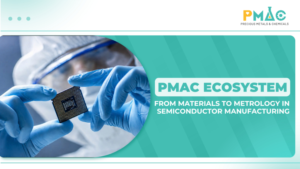
PMAC’s semiconductor technology portfolio includes wafer cleaning and wet-processing equipment, plasma-processing systems, high-purity process chemicals, and related analytical and metrology solutions.
These technology categories support the evaluation of different manufacturing needs, from surface preparation before thin-film deposition to residue removal between fabrication steps and quality assessment after cleaning.
For example, a requirement to remove organic residues after patterning may involve different materials and process conditions from a cleaning operation designed to control particles after CMP. The equipment, chemicals, and inspection strategy therefore need to be considered within the context of each application.
Beyond materials and equipment, PMAC’s technical support framework covers solution consultation, technology integration, installation, commissioning, training, and maintenance.
By connecting these capabilities, PMAC aims to help manufacturers evaluate cleaning solutions as part of their overall fabrication process rather than selecting individual products based solely on equipment specifications.
For a broader view of how these technology categories fit together, explore PMAC’s semiconductor technology ecosystem.
VIII. Frequently Asked Questions About Wafer Cleaning
1. Do New Semiconductor Wafers Need Cleaning Before Use?
Not every new wafer requires the same cleaning procedure. The need for additional treatment depends on the supplier’s cleanliness specifications, packaging conditions, storage environment, and requirements of the next fabrication step. Manufacturers should compare incoming wafer specifications with their process requirements before deciding whether further cleaning is necessary.
2. Can Wafers Become Contaminated Again After Cleaning?
Yes. Contamination can be reintroduced during rinsing, drying, transportation, handling, or storage. The surrounding environment, equipment, contact materials, and time between process steps may all affect wafer surface quality. This is why post-clean handling and environmental control are essential to maintaining the results of the cleaning process.
3. Is Wet Cleaning Better Than Dry Cleaning?
Neither method is universally better. Wet and dry cleaning rely on different mechanisms and have distinct application ranges and limitations. The appropriate choice depends on the contaminants being targeted, materials exposed on the wafer, and the requirements of subsequent fabrication steps.
4. Can One Cleaning Process Be Used Throughout an Entire Semiconductor Production Line?
A single cleaning process generally cannot be applied unchanged to every fabrication stage. Bare wafers and wafers with multiple patterned material layers have different requirements for chemistry, cleaning forces, and surface protection. Each cleaning process must therefore be evaluated for its intended application to ensure contamination is removed without compromising existing structures.
Conclusion
Wafer cleaning plays a critical role in semiconductor manufacturing by controlling contamination, preparing wafer surfaces, and reducing the risk of defects during subsequent fabrication steps.
However, cleaning performance cannot be measured solely by how much contamination is removed. An effective process must also protect existing materials, maintain consistent results, and meet the operational requirements of the manufacturing line.
Contact PMAC to discuss your wafer materials, cleaning objectives, and technical requirements. Our team can help you explore relevant technologies within PMAC’s semiconductor portfolio and evaluate suitable options for your manufacturing application.
PMAC Joint Stock Company
Ho Chi Minh City Office:
4th Floor, HUTECH Building, D1 Road, Saigon Hi-Tech Park, Tang Nhon Phu Ward, Ho Chi Minh City, Vietnam
Hanoi Office:
22B O2, Linh Dam Peninsula, Hoang Liet Ward, Hanoi, Vietnam
Hotline: +84 387 235 878
Facebook: PMAC
Author: PMAC – Nguyen Quoc Dung – Lab & Maintenance Center Chief