

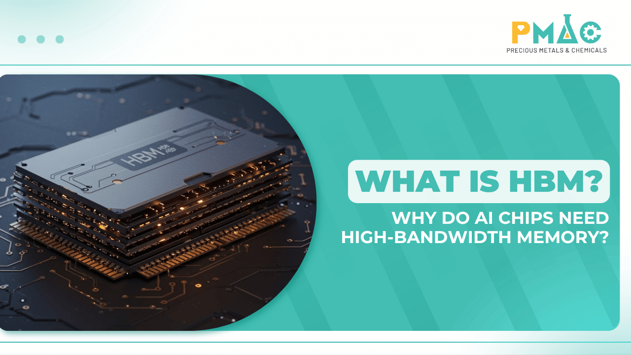
Over the past few years, the explosive growth of artificial intelligence has triggered an unprecedented race in the semiconductor industry. Large Language Models (LLMs), Generative AI, and multimodal AI systems all require the ability to process enormous volumes of data at extremely high speeds. This is precisely why HBM (High Bandwidth Memory) has become one of the most important technologies in modern AI hardware.
HBM fundamentally changes traditional memory architecture by stacking multiple DRAM layers vertically, connecting them through Through-Silicon Via (TSV) technology, and integrating them very close to the GPU using Advanced Packaging.
Thanks to this design, HBM delivers significantly higher bandwidth, lower latency, and better energy efficiency, making it an almost mandatory choice for AI GPUs, AI Accelerators, and high-performance computing (HPC) systems.
So, what exactly is HBM? And why has this technology become so critical for modern AI chips? Let’s take a closer look.
I. What Is HBM?
1. Definition
HBM (High Bandwidth Memory) is a high-bandwidth memory technology designed to handle extremely large data transfers between memory and processors. The HBM standard is developed by JEDEC, the international standards organization for semiconductor memory technologies, and is commercially produced by companies such as SK hynix, Samsung, and Micron.
The key difference between HBM and conventional memory is not the DRAM cell itself, but the way DRAM chips are organized and interconnected. Instead of placing multiple memory chips side by side on a circuit board like DDR or GDDR, HBM stacks multiple DRAM layers vertically to form a memory stack. These layers are connected using TSVs and positioned very close to the GPU within the same package.
This architecture enables HBM to achieve dramatically higher data throughput without requiring extremely high operating frequencies.
2. Why Is It Called “High Bandwidth Memory”?
The term High Bandwidth Memory comes from the primary goal of the technology: increasing Memory Bandwidth, which is the maximum amount of data that memory can transfer to a processor per second.
Memory bandwidth is typically measured in GB/s or TB/s. The higher the bandwidth, the more data a GPU can receive and process within the same period of time.
A simple analogy is:
- Traditional DRAM is like a two-lane road. To increase traffic flow, vehicles must travel faster.
- HBM is like a massive multi-lane highway where thousands of vehicles can travel simultaneously. Even if each vehicle is not moving much faster, the total traffic throughput is dramatically higher.
In other words, HBM does not necessarily rely on the highest clock frequency; instead, it achieves exceptional bandwidth through massively parallel data transfer.
3. Why Is Memory Bandwidth So Important?
In AI systems, GPUs continuously read input data, access model weights, and write computation results back to memory. If memory bandwidth is insufficient, the GPU frequently enters a data-starved state, waiting for data instead of performing computations.
Imagine a factory with thousands of workers. If raw materials are delivered by a single small truck, most workers will spend time waiting rather than producing goods. However, if many trucks deliver materials simultaneously, the factory can operate at full capacity.
In an AI system, the GPU is the factory, while memory bandwidth is the transportation network. Increasing memory bandwidth often improves overall performance more effectively than simply increasing the GPU’s computational power.
II. Why Does AI Need High Bandwidth Memory?
For traditional applications such as web browsing, document editing, or video playback, the amount of data exchanged between memory and the processor is relatively modest. Modern AI workloads are completely different. During every training or inference cycle, the system must access billions of parameters, perform millions of parallel operations, and continuously move data between memory and the GPU.
As a result, memory has become one of the most important factors determining the performance of an AI system.
1. Memory Wall – The Bottleneck of AI Chips
For many years, CPU and GPU performance has improved much faster than memory technology. Chip manufacturers can add more processing cores, increase the number of Tensor Cores, or optimize GPU architectures, but if data cannot be delivered quickly enough, a significant portion of the computational resources remains underutilized.
This gap between processing speed and memory access speed is known as the Memory Wall.
It explains why many GPUs cannot reach their theoretical peak performance despite having enormous computational capability. When data arrives too slowly, GPU cores must wait, reducing hardware utilization and increasing task completion time.
For AI workloads, the Memory Wall becomes even more severe because data volumes grow exponentially.
2. AI Training Requires Massive Memory Bandwidth
AI Training is the most resource-intensive stage of an AI model’s lifecycle. During each training iteration, the GPU must:
- read input data,
- access model weights,
- compute gradients,
- and update billions of parameters.
For large language models, the number of parameters can reach tens or even hundreds of billions. Simply reading and writing these parameters generates an enormous amount of traffic between memory and the GPU.
If memory bandwidth is insufficient, the GPU spends more time waiting for data than performing computations. This not only slows down training but also significantly increases the operating cost of AI data centers.
HBM addresses this problem by providing extremely high bandwidth, allowing GPUs to access far more data within the same amount of time. As a result, training time is reduced and hardware utilization is greatly improved.
3. AI Inference and Generative AI Also Depend on HBM
Not only AI Training, but AI Inference also requires high-bandwidth memory. When a user sends a question to an AI chatbot, the system must continuously load model weights, calculate token probabilities, and generate responses in real time.
Similarly, Generative AI applications such as image, video, and audio generation process large tensors and repeatedly access memory throughout the inference process.
If memory responds too slowly, the GPU must wait for data, increasing response latency and reducing throughput. This is why modern AI GPUs almost universally rely on HBM rather than GDDR.
Beyond large language models, HBM also plays a crucial role in multimodal AI, autonomous vehicles, computer vision systems, and high-performance computing (HPC). The common requirement across these applications is the ability to process enormous amounts of data with very low latency, and HBM provides the bandwidth necessary to keep pace with the rapidly growing performance of modern GPUs.
III. How Does HBM Work?
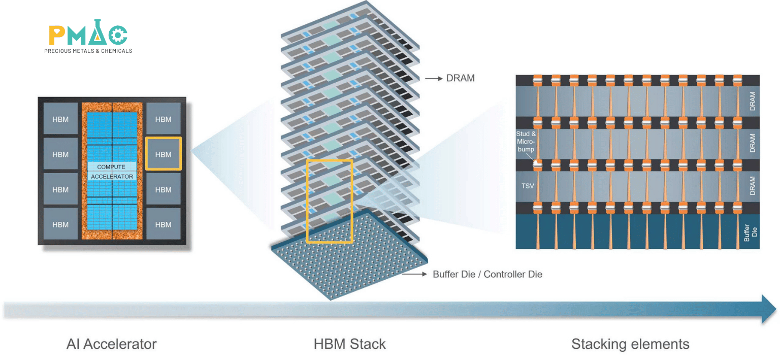
Figure 1: How High Bandwidth Memory (HBM) Works
1. 3D Stacking Architecture
3D Stacking is a technology that vertically stacks multiple DRAM dies to form a single HBM stack. Depending on the HBM generation, one stack may contain 4, 8, 12, or even 16 DRAM layers.
This stacked architecture offers several key advantages:
- Higher memory density: Multiple DRAM dies are integrated within the same footprint, making HBM ideal for AI GPUs that require large memory capacities.
- Shorter signal paths: Data travels only a very short distance between DRAM layers instead of across a printed circuit board (PCB).
- Lower power consumption: Shorter transmission distances reduce the energy required to move data.
- Higher memory bandwidth: Multiple DRAM layers operate in parallel, significantly increasing the amount of data transferred per clock cycle.
Thanks to its 3D stacking architecture, HBM can deliver memory bandwidth measured in terabytes per second, meeting the demands of modern AI GPUs and high-performance computing systems.
2. Through-Silicon Via (TSV)
Through-Silicon Via (TSV) is a vertical electrical interconnection technology that creates microscopic conductive pathways through silicon wafers. After these vias are etched, they are filled with copper (Copper Filling) to form high-speed vertical signal paths between stacked DRAM dies.
By using TSVs, the DRAM layers inside an HBM stack function as a unified memory system. This architecture provides several important benefits:
- Higher interconnect density
- Lower signal latency
- Improved power efficiency
- Massive parallel data transfer with extremely high bandwidth
Today, TSV has become one of the foundational technologies in advanced semiconductor manufacturing. Beyond HBM, it is widely used in many other 3D integration and advanced packaging solutions.
IV. How Does HBM Outperform Conventional Memory?
The primary advantage of HBM lies in its memory architecture, rather than simply increasing operating frequency. Instead of relying on faster signal speeds, HBM uses an extremely wide Wide I/O interface, allowing thousands of data lines to transfer information simultaneously. As a result, significantly more data can be transmitted during each clock cycle.
In addition to its exceptional bandwidth, HBM also consumes less energy per bit of transferred data. This is particularly important for AI data centers, where thousands of GPUs operate continuously around the clock.
DDR vs. GDDR vs. HBM
| Criteria | DDR | GDDR | HBM |
|---|---|---|---|
| Primary Application | PCs, Servers | Graphics Cards | AI GPUs, AI Accelerators, HPC |
| Architecture | 2D | 2D | 3D Stacking |
| Memory Placement | DIMM Module | Around the GPU | On the same package as the GPU |
| Interconnection Technology | PCB | PCB | TSV + Interposer |
| Memory Bandwidth | Moderate | High | Extremely High (TB/s) |
| Latency | Moderate | Low | Low |
| Power Efficiency | Moderate | Good | Excellent |
| Memory Density | Moderate | Moderate | High |
| Scalability | Limited | Good | Excellent |
Each memory technology is designed for a different purpose. DDR is optimized for mainstream PCs and servers, GDDR is designed for consumer graphics cards, while HBM is specifically engineered to provide the ultra-high memory bandwidth required by AI workloads and high-performance computing (HPC).
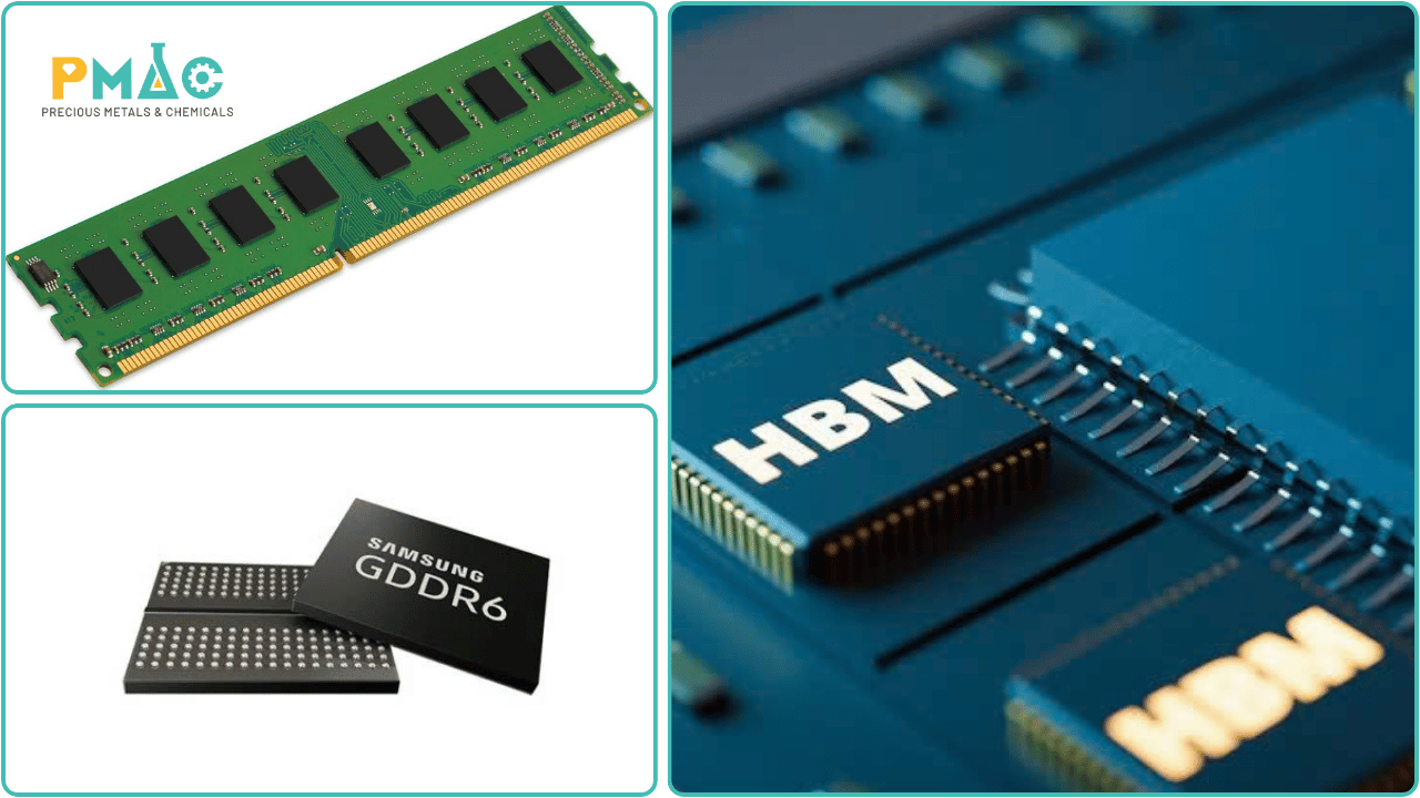
Figure 2: HBM Compared with Conventional DRAM-Based Memory Technologies
V. The Role of Advanced Packaging in HBM
HBM would not be able to achieve its full performance potential through DRAM technology alone. To place memory physically close to the GPU while supporting thousands of high-speed connections, the semiconductor industry relies on Advanced Packaging—a collection of packaging technologies that go far beyond traditional semiconductor assembly methods.
Instead of packaging individual chips separately and connecting them through a printed circuit board, Advanced Packaging integrates the GPU and multiple HBM stacks within the same package. This dramatically shortens signal paths to just a few millimeters—or even less—resulting in higher performance and lower power consumption.
1. Interposer – The Bridge Between the GPU and HBM
A critical component of the HBM architecture is the Interposer. This silicon substrate contains an extremely high-density wiring network and serves as the communication bridge between the GPU and multiple HBM stacks.
With an interposer, data no longer needs to travel across the motherboard. Instead, it moves directly between the GPU and HBM at extremely high speeds, enabling the enormous memory bandwidth that modern AI processors require.
2. Hybrid Bonding and Supporting Technologies
To further improve HBM performance, semiconductor manufacturers are adopting several advanced packaging technologies, including:
- Hybrid Bonding: Directly bonds copper and dielectric surfaces to increase interconnect density while reducing contact resistance.
- Wafer Thinning: Reduces wafer thickness before stacking, lowering the overall height of the memory stack and improving thermal performance.
- Copper Filling: Fills TSV structures with copper to create reliable vertical electrical connections between DRAM layers.
These manufacturing processes require extremely high precision and are carried out using specialized equipment throughout the Semiconductor Manufacturing workflow. This is one of the reasons why HBM is considered among the most sophisticated semiconductor products in production today.
Across the HBM manufacturing ecosystem, advanced solutions such as SABRE 3D, Striker ALD, VECTOR DT, DV-Prime, Coronus, and Syndion are deployed at different stages of production—from TSV formation and thin-film deposition to surface treatment and wafer quality inspection. Together, these technologies improve manufacturing yield while meeting the increasingly stringent requirements of next-generation HBM products.
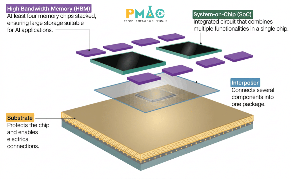
Figure 3: The Role of Advanced Packaging in High Bandwidth Memory (HBM)
VI. The Future of HBM in the AI Era
The rapid advancement of artificial intelligence is accelerating the evolution of High Bandwidth Memory (HBM). Following the introduction of HBM2E, the semiconductor industry has continued to push the boundaries with HBM3 and HBM3E, offering significantly higher memory bandwidth, greater capacity, and improved power efficiency to support next-generation AI GPUs and AI accelerators.
Looking ahead, HBM4 is expected to further enhance performance through wider memory interfaces, taller DRAM stacks, and tighter integration with advanced technologies such as Hybrid Bonding. At the same time, Advanced Packaging is becoming an increasingly important competitive factor in semiconductor manufacturing. As chip performance is no longer determined solely by process nodes, packaging technologies that enable closer integration between processors and memory are playing a critical role in overall system performance.
Demand for HBM is projected to continue growing rapidly, driven by the expansion of AI data centers, cloud computing infrastructure, and Generative AI applications. Beyond GPU manufacturers, memory vendors and semiconductor equipment suppliers are also investing heavily to meet the industry’s increasing demand for advanced HBM solutions.
Read more: PMAC and Precious Metals & Chemicals Company on Vietnam’s Semiconductor Technology Map
Conclusion
HBM is far more than just a faster version of conventional memory. It represents a major architectural advancement that enables modern AI systems to overcome the limitations of the Memory Wall. By combining 3D Stacking, Through-Silicon Via (TSV), and Advanced Packaging, HBM delivers exceptional memory bandwidth, lower latency, and superior energy efficiency compared with traditional memory technologies.
As AI models continue to grow in size and complexity, the importance of HBM will only increase. At the same time, demand for enabling technologies such as Interposer, Hybrid Bonding, Wafer Thinning, and advanced semiconductor manufacturing equipment will continue to rise. In this sense, HBM is not merely a high-performance memory technology—it is a key enabler for the next generation of AI GPUs, AI accelerators, and high-performance computing systems.
PMAC Joint Stock Company
Ho Chi Minh City Office:
4th Floor, HUTECH Building, D1 Road, Saigon Hi-Tech Park, Tang Nhon Phu Ward, Ho Chi Minh City, Vietnam
Hanoi Office:
22B O2, Linh Dam Peninsula, Hoang Liet Ward, Hanoi, Vietnam
Hotline: +84 387 235 878
Facebook: PMAC