

A chip may carry the name of NVIDIA, Qualcomm, Intel, or another semiconductor brand, but that does not mean all the technology inside it was created by a single company. The design may be developed by one company, fabricated on wafers at another facility, and then packaged and tested by a specialized partner. Behind these stages is an even broader network supplying design software, intellectual property, wafers, materials, chemicals, and manufacturing equipment.
This division of roles is not accidental. As chips become more complex, each stage requires deeper technological expertise, greater capital investment, and increasingly specialized know-how. Rather than trying to do everything in-house, the semiconductor industry has evolved into a highly specialized structure with several distinct business models.
That is why terms such as Fabless, Foundry, IDM, and OSAT appear so frequently when discussing the semiconductor value chain. Understanding what Fabless, Foundry, IDM, and OSAT are does more than clarify who designs, manufactures, or packages chips. It also reveals why a modern chip is ultimately the product of an interconnected technology network.
I. Why Has the Semiconductor Industry Developed So Many Different Types of Companies?
At the simplest level, a chip goes through three major stages: design, wafer fabrication, followed by packaging and testing. In practice, however, each of these stages contains many different technologies and specialized processes.
At the design stage, engineers rely on electronic design automation tools to simulate, lay out, and verify circuits. They may also integrate intellectual property blocks developed by other companies. Once a design enters manufacturing, the process requires wafers, high-purity chemicals, thin-film materials, metals, lithography equipment, deposition systems, etching tools, cleaning equipment, and metrology systems. After fabrication is completed on the wafer, the chip still needs to be separated into dies, interconnected, packaged, and tested before it can be integrated into an end product.
This level of specialization allows each company to focus its resources on the capabilities it performs best. TSMC is a clear example. The company follows a specialized foundry model, focusing on manufacturing products for customers rather than competing with them through its own branded chips. In 2025, TSMC reported that it manufactured 12,682 products using 305 different technologies for 534 customers, demonstrating how a manufacturer can serve a vast range of designs without owning those designs itself.
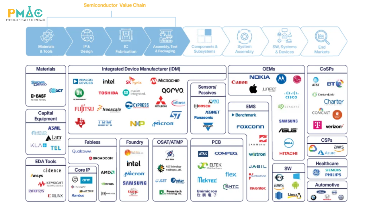
Figure 1. A chip is the result of multiple technology layers and specialized companies across the semiconductor value chain.
II. What Is a Fabless Company, and Why Do Many Major Chipmakers Not Own Fabs?
A Fabless company focuses on chip design and development without owning its own wafer fabrication facility. NVIDIA, AMD, Qualcomm, and MediaTek are familiar examples of this model.
The key characteristic of a Fabless company is not simply that it “does not own a factory.” Designing a high-performance chip is already a highly complex undertaking, while building and operating an advanced semiconductor fab requires an entirely different set of capabilities. By separating these two areas, Fabless companies can focus their resources on chip architecture, features, software, and product development, while fabrication is entrusted to a Foundry with the appropriate infrastructure and process technology.
Even at the design stage, however, Fabless companies rarely create everything from scratch. A chip may incorporate IP – semiconductor intellectual property developed by another company. Arm is a well-known example: its core business is built around licensing IP to semiconductor companies, device manufacturers, and other organizations so they can develop their own chips.
In addition to IP, chip design also depends on EDA – Electronic Design Automation, which supports everything from circuit design and simulation to physical layout and verification before a design is transferred into production. A chip can therefore already incorporate technologies from multiple companies while it still exists only as design data.
III. What Is a Foundry? From Chip Design to High-Volume Wafer Production
If Fabless companies focus on how a chip should be designed, a Foundry addresses the challenge of turning that design into a physical product with sufficient stability for high-volume manufacturing.
A Foundry owns semiconductor fabrication capabilities and manufactures chips based on customer designs. TSMC is one of the clearest examples of a pure-play foundry. The company focuses on manufacturing technology and production services for customers rather than developing its own chips that would compete directly with them. This model has enabled Fabless companies to grow without having to invest in their own network of fabrication facilities.
A Foundry, however, does not simply receive a design file and “print” it onto a wafer. To form transistors and interconnect layers, wafers must pass through repeated processes including thin-film deposition, lithography, etching, doping, thermal processing, and metallization. Even a small variation in film thickness, dimensions, composition, or defect level can affect the number of good dies produced on each wafer.
The value of a Foundry therefore lies in more than owning a fab. The ability to maintain process stability, control defects, and achieve sufficiently high yield ultimately determines whether a design can enter commercial production at a viable cost.
Even a large Foundry cannot develop every technology required inside its fab. TSMC operates its Grand Alliance, connecting customers with EDA providers, IP companies, design partners, packaging providers, and equipment and materials suppliers. This reflects the real structure of the industry: owning a fab does not mean owning every technology that supports it.
IV. What Is an IDM? When Design and Manufacturing Are Combined Within One Company
IDM – Integrated Device Manufacturer refers to a business model in which a company both designs semiconductor products and owns fabrication capabilities. Intel, Texas Instruments, Infineon, Micron, and SK hynix are commonly cited examples.
Compared with a Fabless company, an IDM has more direct control over multiple stages of chip development. Device design can be optimized alongside materials and manufacturing technology within the company’s own fabs. For products that require tight coordination between device structures and manufacturing processes, this level of integration can provide a significant advantage.
However, being an IDM does not mean doing everything internally. An IDM still relies on EDA tools, IP, manufacturing equipment, chemicals, materials, metrology systems, and many technologies supplied by external partners. Where appropriate, it may also use external Foundries for certain products or process technologies.
Intel demonstrates how these boundaries are becoming increasingly flexible. In addition to designing and manufacturing its own chips, the company is developing Foundry services for external customers. In its latest reporting, Intel describes its Foundry capabilities as extending beyond wafer fabrication to include advanced packaging, chiplet integration, and design enablement, supported by an ecosystem of EDA tools, process design kits, and IP that customers need to use Intel’s technologies.
V. What Is OSAT, and Why Is a Chip Still Not Finished When It Leaves the Wafer Fab?
Once wafer fabrication is complete, the chip is still not ready to be placed directly into a smartphone, vehicle, or server. Dies must be separated from the wafer, electrically interconnected, packaged, and tested to ensure they meet performance and reliability requirements.
This is the role of OSAT – Outsourced Semiconductor Assembly and Test, referring to companies specializing in semiconductor assembly, packaging, and testing services. Amkor, ASE, and JCET are among the best-known companies in this segment. Amkor is one of the major providers of outsourced semiconductor packaging and test services, allowing customers to focus their resources on design and wafer fabrication while Amkor handles packaging and testing technologies.
Packaging was once often viewed as a downstream step. The rise of chiplets, HBM, and 2.5D/3D integration is changing that role. When multiple dies must be placed side by side or stacked within the same package, packaging design begins to directly influence signal paths, power delivery, thermal behavior, and overall system performance.
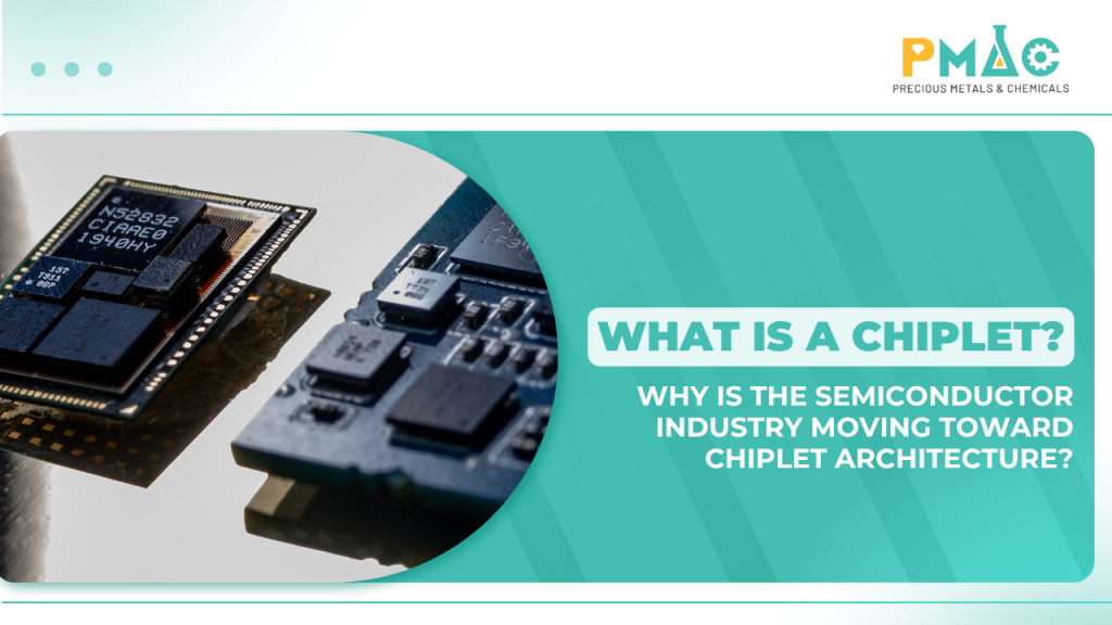
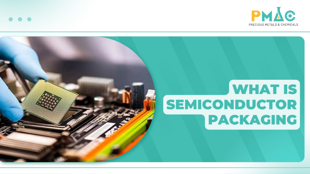
As a result, semiconductor packaging is no longer simply about “protecting the chip.” It is increasingly becoming part of the system architecture itself. PMAC has explored this shift in greater detail in What Is Semiconductor Packaging? and What Is a Chiplet?.
The scale of this back-end segment also reflects the growing importance of OSAT. According to SEMI’s July 2026 database, more than 820 assembly and test facilities operated by IDMs and OSAT companies are being tracked globally, with coverage extending to advanced packaging, substrates, and interposers.
VI. How Do Fabless, Foundry, IDM, and OSAT Differ?
After understanding the role of each business model, the differences among the four can be summarized as follows:
| Model | Primary Role | Advantages | Limitations | Representative Companies |
| Fabless | Designs and develops chips while outsourcing fabrication | Can focus resources on architecture, design, and product development; avoids the capital burden of building and operating fabs; can choose among manufacturing technologies | Depends on Foundry capacity, capability, and production schedules; has less direct control over fabrication; more exposed to supply-chain disruptions | NVIDIA, AMD, Qualcomm, MediaTek |
| Foundry | Manufactures chips based on customer designs | Deep specialization in manufacturing technology; can utilize fabs efficiently by serving many customers; able to invest heavily in advanced process technologies | Extremely high fab construction and operating costs; must maintain high yield; strongly dependent on equipment, materials, and customer demand | TSMC, UMC, GlobalFoundries |
| IDM | Designs and fabricates chips within the same company | Tighter control between design and manufacturing; can optimize products around proprietary process technologies; greater control over certain critical stages | Very high capital and operating requirements; must maintain both design and manufacturing capabilities; still depends on many external suppliers | Intel, Texas Instruments, Infineon |
| OSAT | Provides semiconductor assembly, packaging, and testing | Deep specialization in post-wafer processes; serves many customers and package formats; increasingly important in advanced packaging | Depends on customer wafers/dies as well as substrate and material supply; must support many packaging architectures; has less control over core chip design | ASE, Amkor, JCET |
The table shows that no single model is superior in every respect. Fabless companies reduce the burden of fab investment but depend more heavily on Foundries. IDMs gain greater control over multiple stages but must carry substantial capital and operating costs. Foundries benefit from deep specialization in manufacturing, while OSAT companies focus on packaging and testing, areas that are becoming increasingly critical for modern chips.
These trade-offs explain why the semiconductor industry has not evolved toward a structure where every company tries to do everything itself. Instead, companies increasingly develop deep expertise in a limited number of core capabilities and connect with specialized partners for the rest.
Fabless, Foundry, IDM, and OSAT still do not represent the entire picture. Before a chip is manufactured, companies need EDA and IP. Inside the fab, they also depend on materials, chemicals, equipment, and metrology technologies. These additional layers help explain why the semiconductor value chain operates more like an ecosystem than a simple production line.
VII. EDA and IP Enter the Process Before the Chip Ever Reaches a Fab
A modern chip may contain billions of transistors, making it virtually impossible to design every structure manually. EDA tools are used for simulation, layout, timing analysis, circuit verification, and design validation before data is transferred into manufacturing.
EDA tools, however, do not operate independently of the Foundry. Every fabrication process has its own limits and design rules, so design tools must be developed and validated for compatibility with the manufacturing technology. TSMC states that partners in its EDA Alliance work directly with its technology teams to develop tools suited to each generation of process technology.
IP plays a similar role. Instead of redesigning every processor, interface, or functional block from scratch, semiconductor companies can use pre-developed and pre-verified IP blocks. This can shorten development time, but it also makes compatibility among IP, EDA, and Foundry technology increasingly important.
That is why large Foundries provide more than fabrication capability. TSMC’s Open Innovation Platform connects EDA, IP, design services, cloud infrastructure, packaging, and other partners so a design can move from an idea to actual silicon.
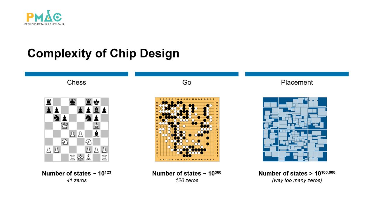
Figure 2. The complexity of chip placement illustrates why modern semiconductor design relies on EDA tools.
VIII. Materials and Equipment Form the Infrastructure Behind the Entire Semiconductor Industry
If Fabless companies create the design and Foundries turn that design into wafers, another question follows: where does the manufacturing technology inside the fab come from?
A fab requires wafers and substrates, high-purity chemicals, gases, deposition precursors, lithography materials, metallization materials, and chemicals for cleaning and polishing. At the same time, the entire process depends on deposition, etching, thermal processing, cleaning, plating, inspection, and metrology equipment.
These layers are tightly interconnected. A material change may require different process conditions. A new equipment technology may require different materials. Metrology systems must also be sensitive enough to confirm that the process remains within its control limits. Therefore, materials, equipment, processes, analysis, and metrology cannot be treated as completely independent categories.
This is also the direction PMAC is developing in the semiconductor sector: connecting materials, equipment, analytical and metrology solutions, and technical support around specific manufacturing challenges rather than treating each product category separately. This approach forms part of the broader PMAC industrial ecosystem.
The relationship is particularly clear in processes such as metallization. Bath composition, process conditions, and metal-layer thickness can all influence the electrical characteristics and stability of a device. PMAC has discussed this topic in greater depth in Semiconductor Plating Materials.
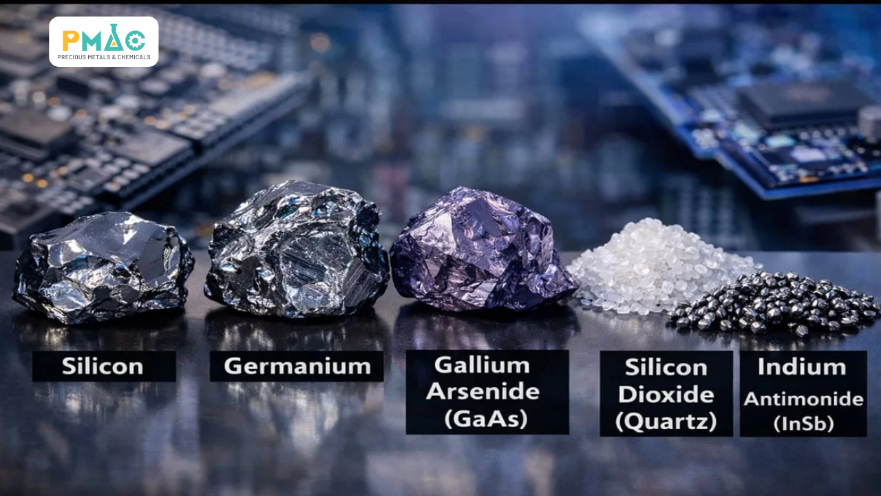
Figure 3. The semiconductor industry uses multiple material systems, each serving different technical requirements and applications.
IX. The Boundaries Between Semiconductor Business Models Are Becoming Less Distinct
The Fabless–Foundry–IDM–OSAT structure remains very useful for understanding the industry, but the reality today is more complex than the traditional classification suggests. Foundries are no longer limited to wafer fabrication. Technologies such as chiplets and 2.5D/3D packaging are pushing major Foundries to expand into advanced packaging and system integration. IDMs may use external Foundries for certain products, while OSAT companies increasingly need to participate earlier in product development to address packaging, substrate, thermal, and testing requirements.
This trend is even more visible in AI chips. A processor may contain multiple chiplets fabricated using different process technologies and then integrated with HBM in a package with extremely high interconnect density. At that point, logic design, memory, substrate, package architecture, and thermal management can no longer be decided independently.
TSMC reflects this shift through its 3DFabric Alliance, an ecosystem that connects EDA, IP, memory, OSAT, substrates, and testing to support 3D IC design and system-level integration. The important point is that the semiconductor value chain can no longer be easily visualized as a simple sequence of design → manufacturing → packaging. As chips become more complex, it is increasingly becoming a co-development network, where multiple companies must exchange technical requirements from the earliest stages.
X. Why Can’t Any Semiconductor Company Make an Entire Chip on Its Own?
The reason is not simply that “chip manufacturing is too complex.” More precisely, each technology layer within the industry has become specialized enough to function as a distinct capability of its own.
Fabless companies may focus on architecture and products, but they still need EDA, IP, Foundries, and OSAT partners. Foundries own fabs but depend on equipment, materials, design tools, and customer ecosystems. IDMs control more stages internally but still rely on a broad external supplier network. OSAT companies must also coordinate with designers, wafer suppliers, substrate providers, material suppliers, and test-system companies to support increasingly sophisticated package architectures.
The strength of a semiconductor company therefore does not depend only on how many technologies it owns internally. The ability to connect the right technologies, suppliers, and partners at each stage is increasingly becoming part of competitive capability itself.
This perspective is also important for companies seeking to participate in the semiconductor supply chain. Opportunities do not necessarily begin with designing or fabricating an entire chip. Companies can create value in wafers, materials, equipment, packaging, analysis, metrology, or highly specialized process steps that are essential to keeping the broader manufacturing system stable.
A chip may therefore carry only one commercial name on the outside, but behind it stands a global technology network. As chip architectures continue to become more complex, the role of that network will only grow.
PMAC Joint Stock Company
Ho Chi Minh City Office:
4th Floor, HUTECH Building, D1 Road, Saigon Hi-Tech Park, Tang Nhon Phu Ward, Ho Chi Minh City, Vietnam
Hanoi Office:
22B O2, Linh Dam Peninsula, Hoang Liet Ward, Hanoi, Vietnam
Hotline: +84 387 235 878
Facebook: PMAC