

A modern semiconductor chip is built from numerous material layers with different functions, created and processed sequentially on the wafer surface. Some layers conduct electricity, others provide insulation or prevent material diffusion between adjacent layers, while certain films directly influence how a transistor controls electrical current. Creating the correct material is therefore only the beginning; manufacturers must also tightly control the thickness, uniformity, composition, and properties of each layer.
These requirements become increasingly demanding as chip structures evolve from planar designs to FinFET, Gate-All-Around (GAA) transistors, and 3D NAND. Films that once needed to cover relatively simple surfaces must now extend into deep trenches, wrap around three-dimensional structures, or maintain extremely small thicknesses across complex geometries. In this context, PVD – Physical Vapor Deposition, CVD – Chemical Vapor Deposition, and ALD – Atomic Layer Deposition have become three important thin-film deposition technologies in semiconductor manufacturing.
I. Thin Films in Semiconductor Manufacturing
1. What Is a Thin Film?
In semiconductor manufacturing, a thin film is a layer of material formed on a wafer with controlled thickness and properties to perform a specific technical function. Depending on its position within the chip structure, the film may consist of conductive metals such as copper, aluminum, or tungsten; insulating materials such as silicon dioxide and silicon nitride; diffusion barriers such as TiN or TaN; or high-k dielectric materials used in advanced transistors.
These layers do not function independently. A metal layer may require a diffusion barrier underneath to prevent material migration into adjacent layers, while a dielectric layer must possess suitable electrical properties to isolate conductive regions. As a result, the quality of one thin film can directly affect the next manufacturing step and ultimately influence chip performance, reliability, and yield.
2. What Is Deposition Technology?
The process of placing material onto a wafer to form these thin films is known as deposition. During semiconductor fabrication, deposition is performed repeatedly and alternates with processes such as photolithography, etching, cleaning, thermal treatment, and metrology. Each cycle adds or shapes part of the device structure until the transistor and electrical interconnect system are completed.
PMAC has also discussed this manufacturing structure in the article What Are Fabless, Foundry, IDM, and OSAT? Why Does No Semiconductor Company Make an Entire Chip on Its Own?, where semiconductor fabrication is described as a sequence of repeated processes including deposition, photolithography, etching, doping, thermal processing, and metallization.
Among the most widely discussed and applied deposition methods are PVD, CVD, and ALD. Their main differences lie in how material is delivered to the wafer surface and how the film is formed. PVD relies on a physical process, while CVD and ALD form films through chemical reactions involving precursors. These different mechanisms give each technology its own strengths and limitations.
3. Technical Requirements for Thin-Film Deposition
When semiconductor devices were larger and the surfaces being coated were relatively flat, deposition requirements focused mainly on producing stable, uniform films at high throughput. As transistor dimensions have continued to shrink, however, diffusion barriers, dielectric layers, and other functional films have also become thinner, while three-dimensional device architectures have made the surfaces being coated increasingly complex.
Modern deposition technology therefore needs to balance several requirements at the same time, including material purity, film thickness, wafer-level uniformity, the ability to coat the sidewalls and bottoms of deep structures, processing speed, and the thermal limits of materials already present on the wafer. No single deposition method can optimize all of these requirements. Semiconductor fabs therefore continue to use multiple deposition technologies in parallel to achieve the required manufacturing performance.
II. Physical Vapor Deposition (PVD)
1. PVD Process
Physical Vapor Deposition (PVD) refers to a group of methods in which a source material is physically converted into a vapor before being deposited onto a wafer. In semiconductor manufacturing, one of the most widely used PVD techniques is sputtering, where plasma is generated in a vacuum environment and energetic ions collide with a solid source known as a target.
These collisions eject atoms from the target surface. The atoms then travel through the vacuum chamber toward the wafer and condense on its surface to form a thin film. Applied Materials describes semiconductor PVD as a process in which material is vaporized from a target through sputtering or evaporation and subsequently condensed on the wafer surface.
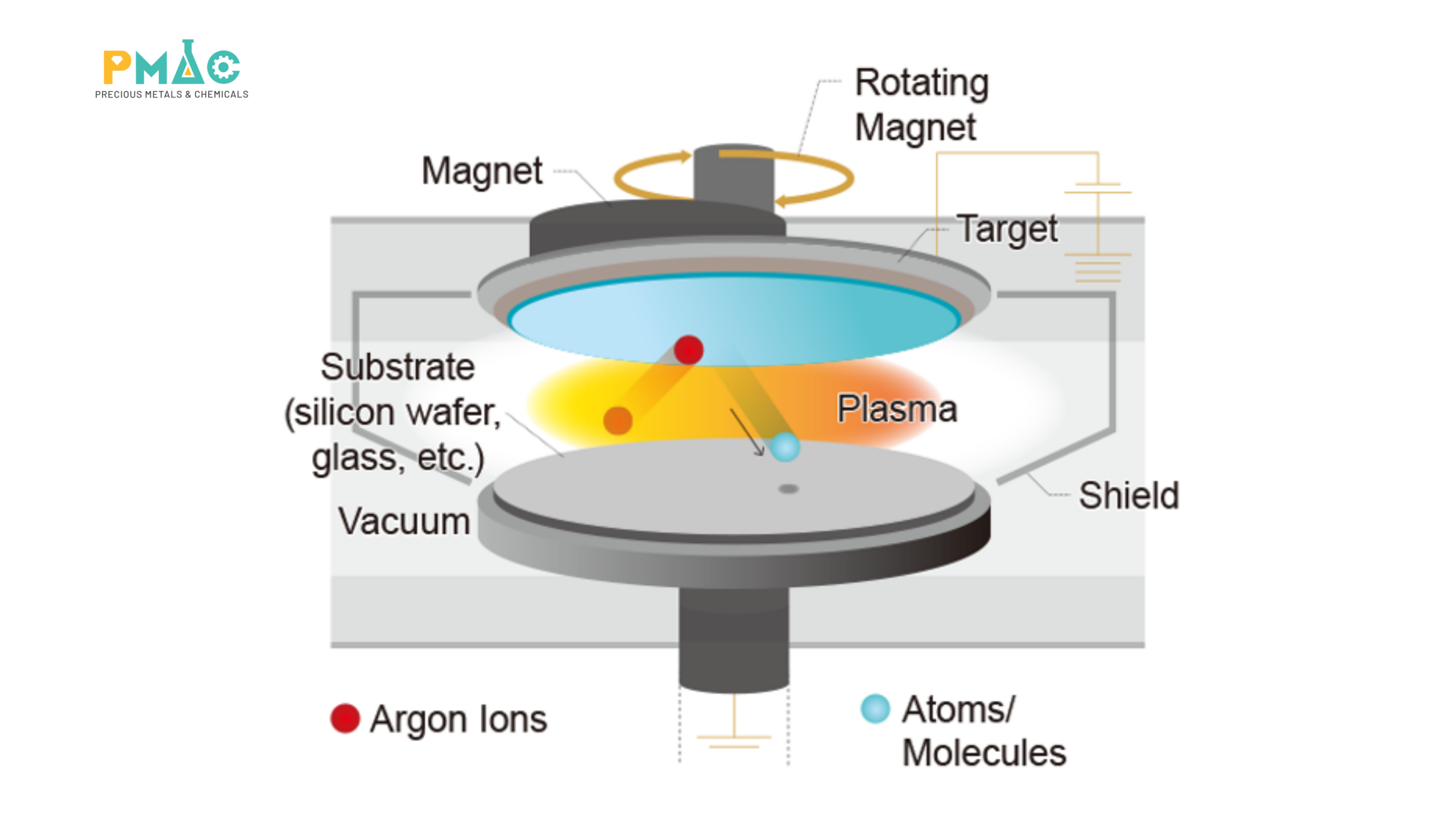
Figure 1. Principle of PVD using the sputtering method
2. Role of PVD
PVD plays a particularly important role in metallization, as it is well suited to depositing many types of high-purity metal and metal nitride films. Common applications include aluminum metallization, Ti/TiN liners, diffusion barriers, and barrier/seed layers for copper interconnect systems.
This makes the quality of the PVD target an important part of the manufacturing process. The chemical composition, purity, and uniformity of the target can influence film composition, defect density, and wafer-to-wafer process stability. PVD is therefore often selected when the primary requirement is to create clean, well-controlled metallic films efficiently.
3. Limitations of PVD
The limitations of PVD become more apparent as wafer structures become increasingly complex. Material atoms travel from the target toward the wafer along relatively directional paths, which can cause uneven material distribution between the top surface, sidewalls, and bottom of a deep feature.
In structures with a high aspect ratio, maintaining a continuous and uniform film becomes more difficult. As semiconductor architectures continue to shrink and become more three-dimensional, there is increasing demand for deposition methods in which materials can reach complex surfaces through chemical reactions rather than primarily directional physical transport.
III. Chemical Vapor Deposition (CVD)
1. CVD Process
Chemical Vapor Deposition (CVD) forms thin films through chemical reactions involving precursors introduced into the process chamber as gases or vapors. When these precursors reach the wafer under appropriate temperature, pressure, and energy conditions, they react or decompose on the surface to form the desired material, while gaseous by-products are removed from the chamber.
Unlike PVD, the final material is not transferred directly from a solid target to the wafer. Instead, the film is created directly on the surface through a controlled sequence of chemical reactions. According to Applied Materials, CVD exposes the substrate surface to one or more volatile precursors that react or decompose to form the required film.
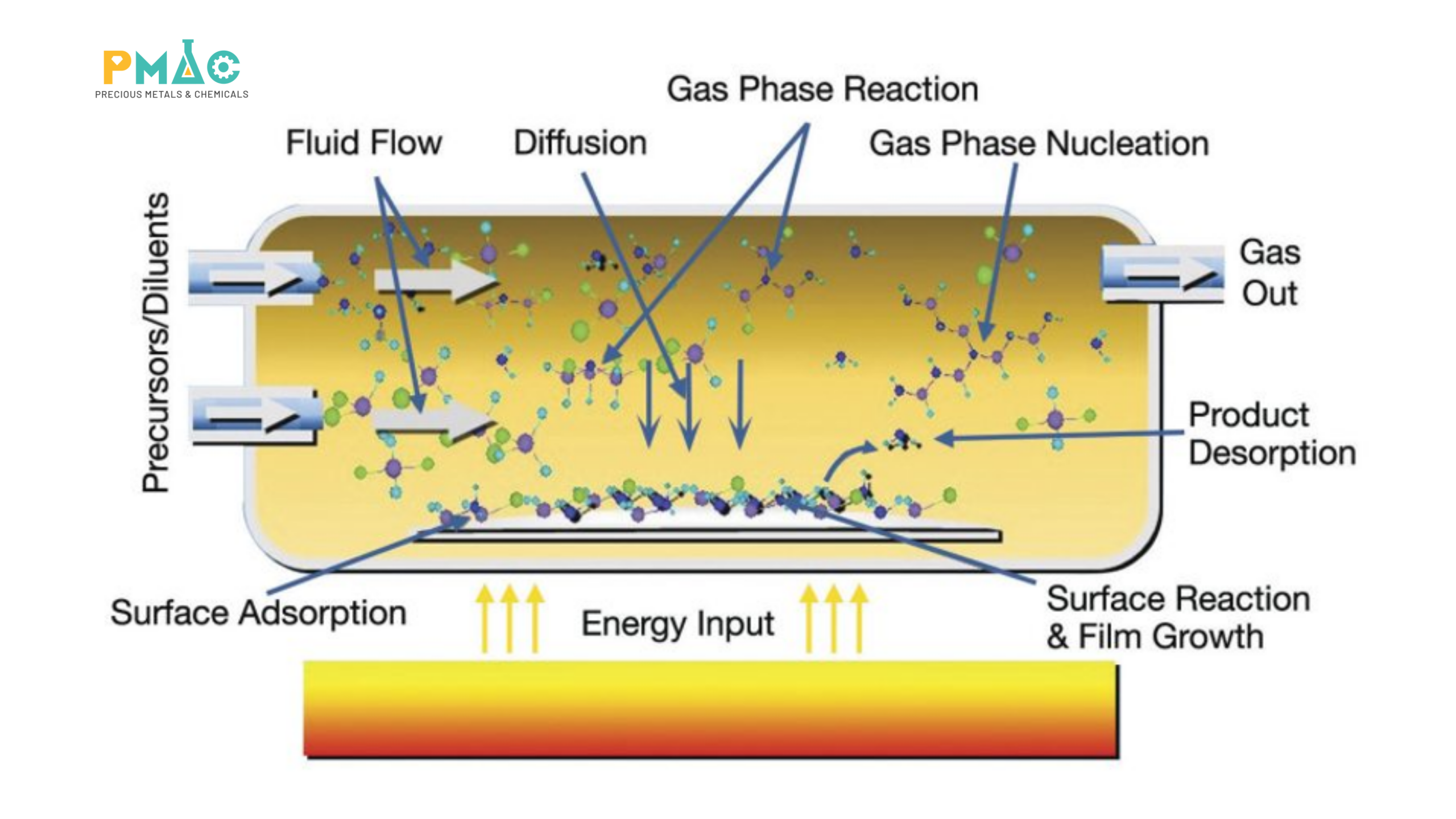
Figure 2. Principle of Chemical Vapor Deposition
2. Role of CVD
The ability to use a wide variety of precursors gives CVD a broad material range. It is used to deposit oxides, nitrides, silicon, tungsten, low-k dielectric materials, and many other functional films used in transistors, interconnect systems, memory devices, and specialized semiconductor components.
CVD can also provide better surface coverage than PVD in many applications because gaseous precursors can access areas that are more difficult for directional material transport to reach. CVD is widely used today in logic, DRAM, NAND, MEMS, photonics, and power semiconductor applications.
3. PECVD
An important variation of CVD is Plasma-Enhanced Chemical Vapor Deposition (PECVD). In PECVD, plasma supplies additional energy to activate or accelerate chemical reactions, allowing many deposition processes to operate at lower temperatures than conventional thermal CVD.
This becomes especially important when the wafer already contains materials that cannot tolerate further high-temperature processing. PECVD therefore expands the application range of CVD in processes with a limited thermal budget, while still maintaining deposition rates suitable for high-volume manufacturing. Industrial PECVD platforms are currently used to deposit various oxides, nitrides, and other materials across different generations of semiconductor devices.
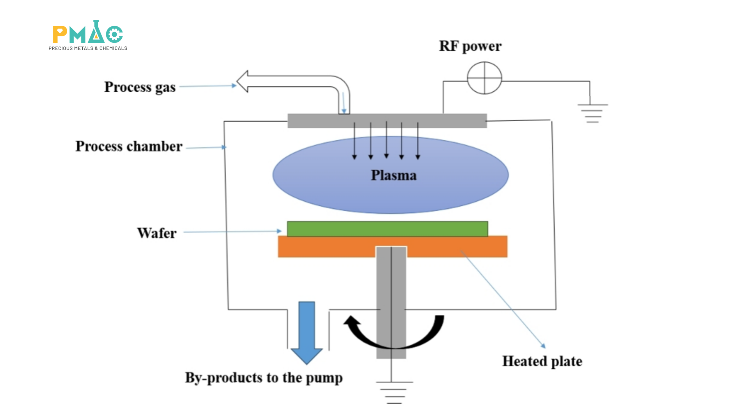
Figure 3. Principle of Plasma-Enhanced Chemical Vapor Deposition (PECVD)
4. Limitations of CVD
Although CVD can provide better coverage than PVD in many applications, its performance still depends heavily on precursor chemistry, temperature, surface reaction rates, and gas transport within the structure. When trenches become very deep and narrow, precursors may react or become depleted before reaching lower regions uniformly.
Thickness control also becomes more challenging when extremely thin films are required. Because conventional CVD reactions are generally continuous, applications requiring very tight control at extremely small dimensions and highly conformal coatings over complex three-dimensional structures may benefit from a sequential reaction mechanism such as ALD.
IV. Atomic Layer Deposition (ALD)
1. ALD Process
Atomic Layer Deposition (ALD) also relies on chemical reactions involving precursors, but the reactants are introduced into the chamber sequentially rather than simultaneously. One precursor first reacts with the surface, after which excess precursor and reaction by-products are removed through a purge step before the next reactant is introduced.
The defining feature of ALD is its self-limiting reaction mechanism. Once the available reaction sites on the surface become saturated, supplying additional precursor does not significantly increase film growth until the next reaction step begins. By repeating these cycles, film thickness can be controlled with very high precision. ASM describes ALD as a surface-controlled, layer-by-layer process capable of highly precise deposition of ultrathin films.
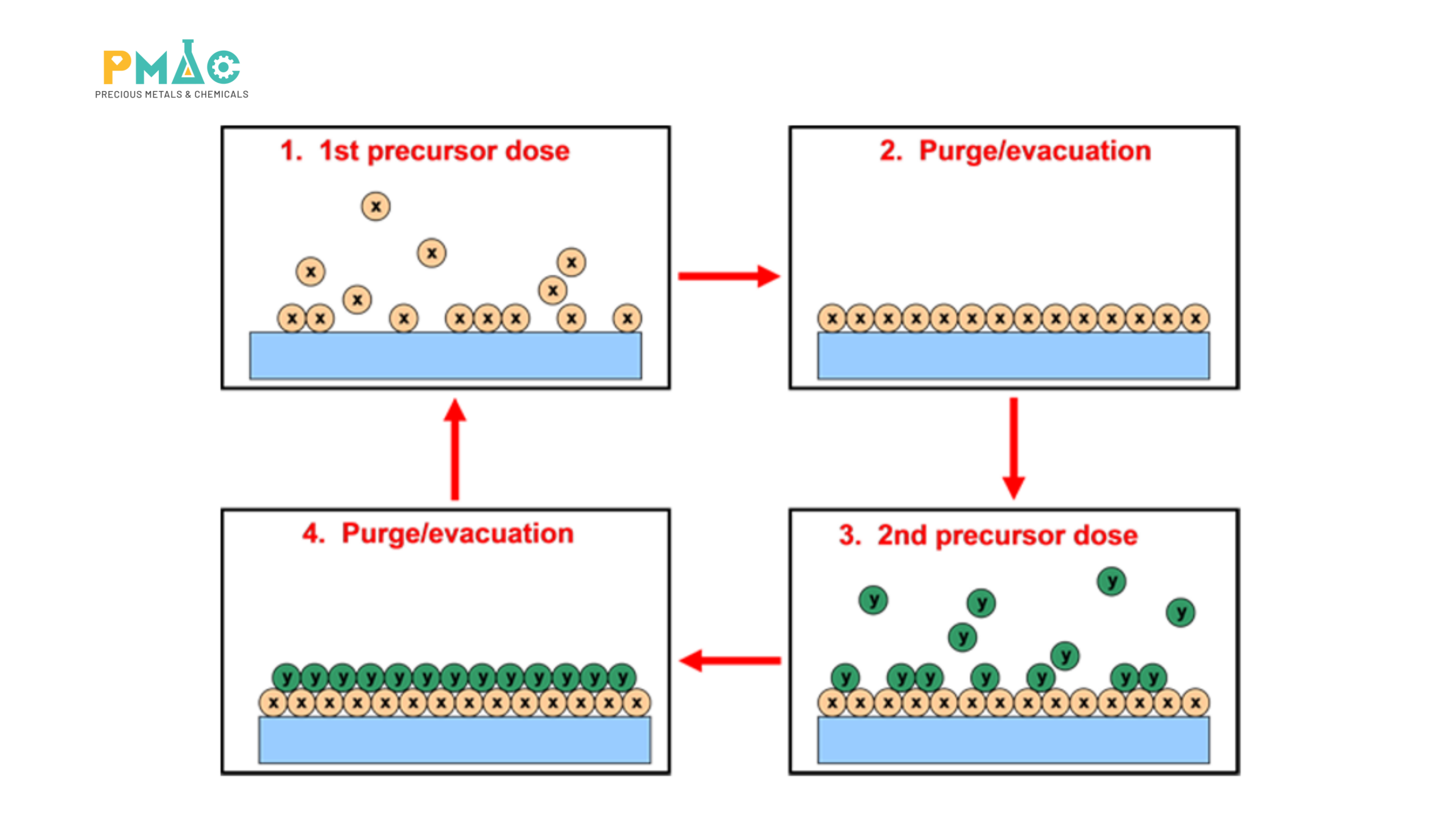
Figure 4. Atomic Layer Deposition (ALD) cycle
2. Role of ALD
ALD becomes particularly valuable when semiconductor manufacturers need to create extremely thin and highly uniform films on increasingly complex structures. Because the reaction takes place directly at the surface, the film can cover the top, sidewalls, and bottom of three-dimensional structures more effectively than strongly directional deposition methods.
ALD is currently used for high-k dielectric layers, diffusion barriers, liners, spacers, metal–insulator–metal capacitors, and numerous applications in logic, DRAM, 3D NAND, and advanced packaging. ASM identifies the ability to form ultrathin, uniform films with excellent coverage over complex structures as one of the core advantages of ALD.
3. What Is Conformality?
An important concept associated with ALD is conformality, which refers to the ability of a deposited film to maintain relatively uniform thickness and properties across surfaces with different orientations, including top surfaces, vertical sidewalls, and the bottoms of deep trenches.
Conformality becomes especially important as chip architectures move toward three-dimensional structures. Gate-All-Around transistors, DRAM capacitors, and 3D NAND may contain very deep and narrow features where films must remain continuous and maintain similar properties throughout the structure. This ability to control thin films across complex geometries is one of the main reasons ALD is becoming increasingly important in advanced logic and memory manufacturing.
4. Limitations of ALD
The high precision of ALD comes with greater process complexity. Each cycle requires multiple precursor dosing, purging, and reaction steps, which must be repeated until the desired film thickness is achieved. As a result, throughput is generally lower than that of continuous deposition methods, particularly when relatively thick films are required.
ALD performance also depends on identifying precursors with the necessary purity, stability, volatility, and reactivity for self-limiting surface reactions. The technology therefore provides the greatest value in applications where tight thickness control and conformal coverage justify the additional process complexity and processing time.
V. The Evolution of Thin-Film Deposition Technology
1. Device Scaling
As transistor dimensions decrease, the space available for diffusion barriers, dielectric layers, and electrical interconnects also becomes smaller. A film that is too thick can consume space needed for the conductive path, while a film that is too thin or discontinuous can increase the risk of leakage, material diffusion, or reduced reliability.
The deposition challenge is therefore shifting from simply creating the correct material to controlling that material at increasingly smaller dimensions. Variations that may once have been acceptable become significant when total film thickness is reduced to extremely small scales.
2. Three-Dimensional Architectures
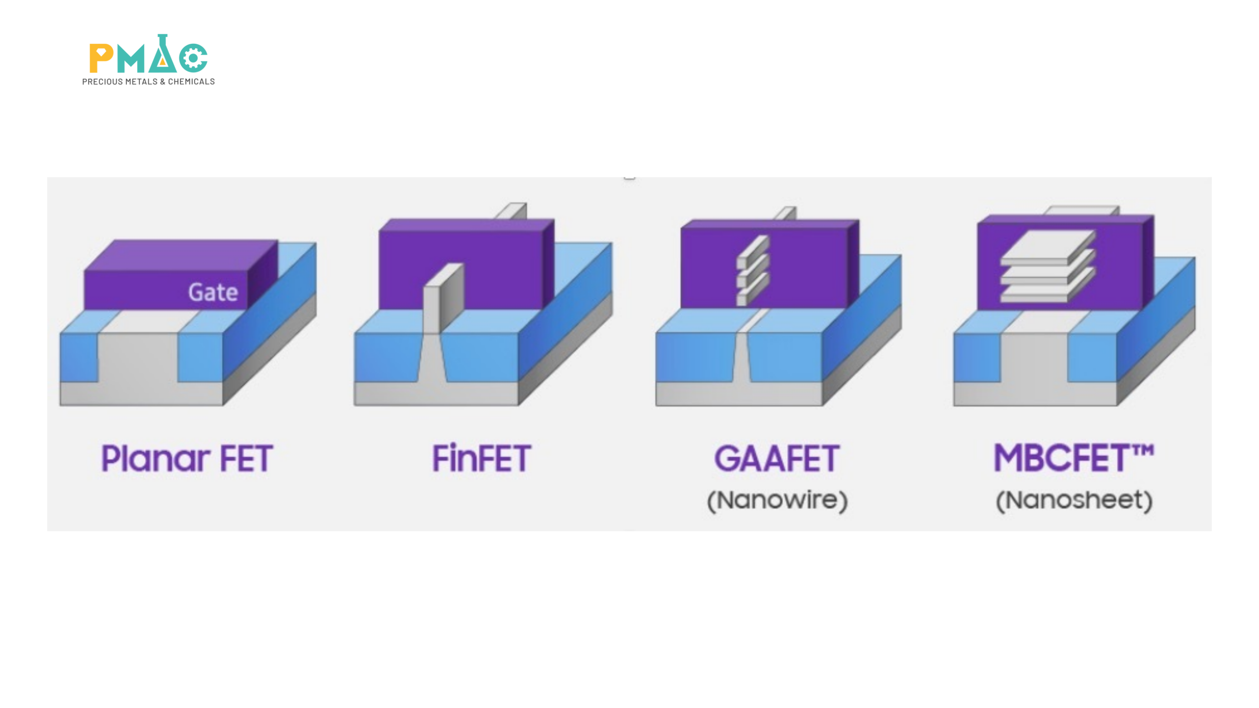
Figure 5. Evolution from planar transistors to three-dimensional transistor architectures
The transition from planar transistors to FinFET and Gate-All-Around architectures, together with the development of 3D NAND, has significantly changed the geometry of the surfaces that must be coated. Wafers increasingly contain vertical sidewalls, cavities, trenches, and structures with high aspect ratios rather than predominantly flat regions.
This trend increases demand for deposition technologies capable of maintaining strong surface coverage and high conformality. The development of three-dimensional architectures is also one of the factors driving the growing importance of ALD in advanced semiconductor manufacturing.
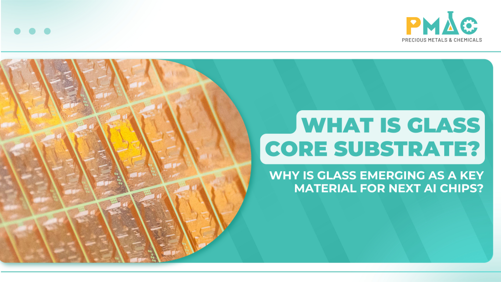
At a broader level, the move toward three-dimensional device structures and increasingly complex packaging is reshaping the semiconductor technology chain. PMAC has discussed part of this trend in the article What Is a Glass Core Substrate? Why Is Glass Being Considered for Next-Generation AI Chips?, which examines materials, metallization, and metrology in the context of advanced packaging.
3. Metrology and Process Control
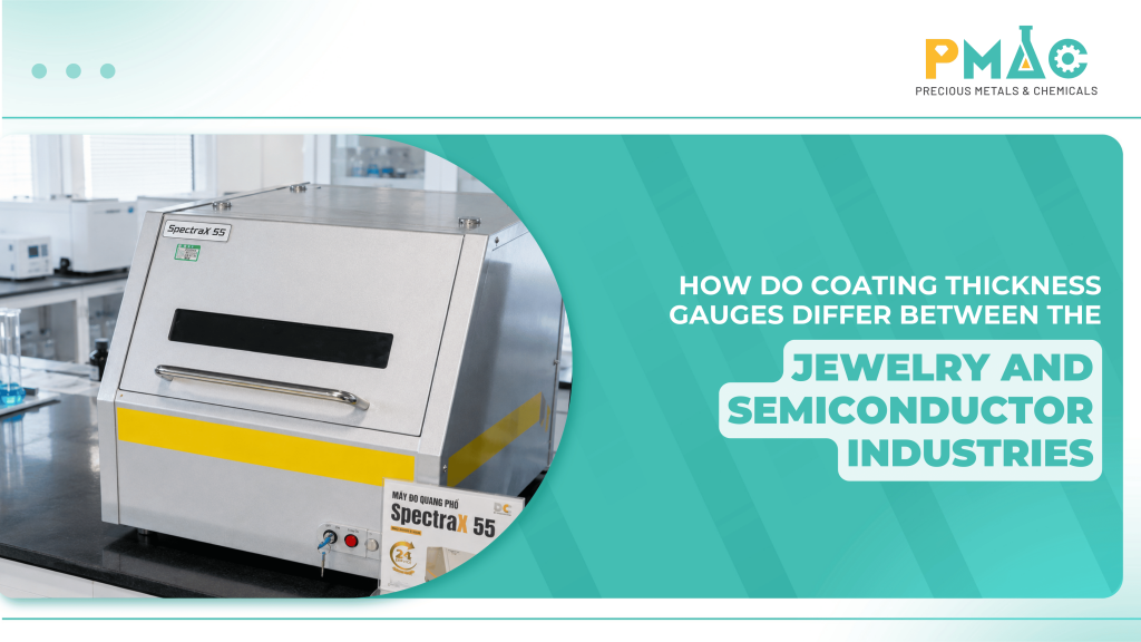
After deposition, manufacturers need to verify whether the actual film meets design requirements through measurements of thickness, composition, uniformity, electrical resistance, and other material properties. Thin-film deposition is therefore closely connected with metrology, process control, and materials analysis.
This relationship becomes even more important as process windows become narrower. A highly precise deposition system delivers limited value if the manufacturer cannot measure and verify the resulting film after each stage. Metrology data provides the basis for adjusting process parameters, monitoring process drift, and maintaining consistency from wafer to wafer.
VI. Comparison of PVD, CVD, and ALD
| Criteria | PVD | CVD | ALD |
| Film formation mechanism | Physical process from a material target | Continuous chemical reaction of precursors | Sequential, self-limiting chemical reactions |
| Material source | Solid target | Gaseous or vapor-phase precursors | Gaseous or vapor-phase precursors supplied sequentially |
| Thickness control | Good | Good | Very high |
| Deep-structure coverage | More limited | Good in many applications | Very good |
| Conformality | Lower | Fair to good, depending on the process | Very high |
| Deposition rate | Generally high | Generally high | Lower due to cyclic growth |
| Typical materials | Metals, metal nitrides | Oxides, nitrides, silicon, tungsten, dielectric materials | High-k dielectrics, oxides, nitrides, barriers, and ultrathin films |
| Main applications | Metallization, liners, barriers, seed layers | Dielectrics, gap fill, low-k materials, functional films | High-k gate, GAA, DRAM, 3D NAND, liners, barriers |
| Main limitations | Limited coverage of deep structures | Dependence on precursor chemistry, thermal limits, and precursor transport | Lower throughput and stricter requirements for precursors and process cycles |
The three methods reflect different technical priorities in semiconductor manufacturing. PVD is well suited to many metallic films and applications requiring relatively high deposition rates. CVD provides a strong balance between material flexibility, surface coverage, and throughput, while ALD is preferred when film thickness and conformality become the dominant requirements. The development of ALD therefore does not replace PVD or CVD; instead, it adds another essential tool for structures that the other two methods may not optimally address.
VII. Materials and Process Control
1. PVD Targets
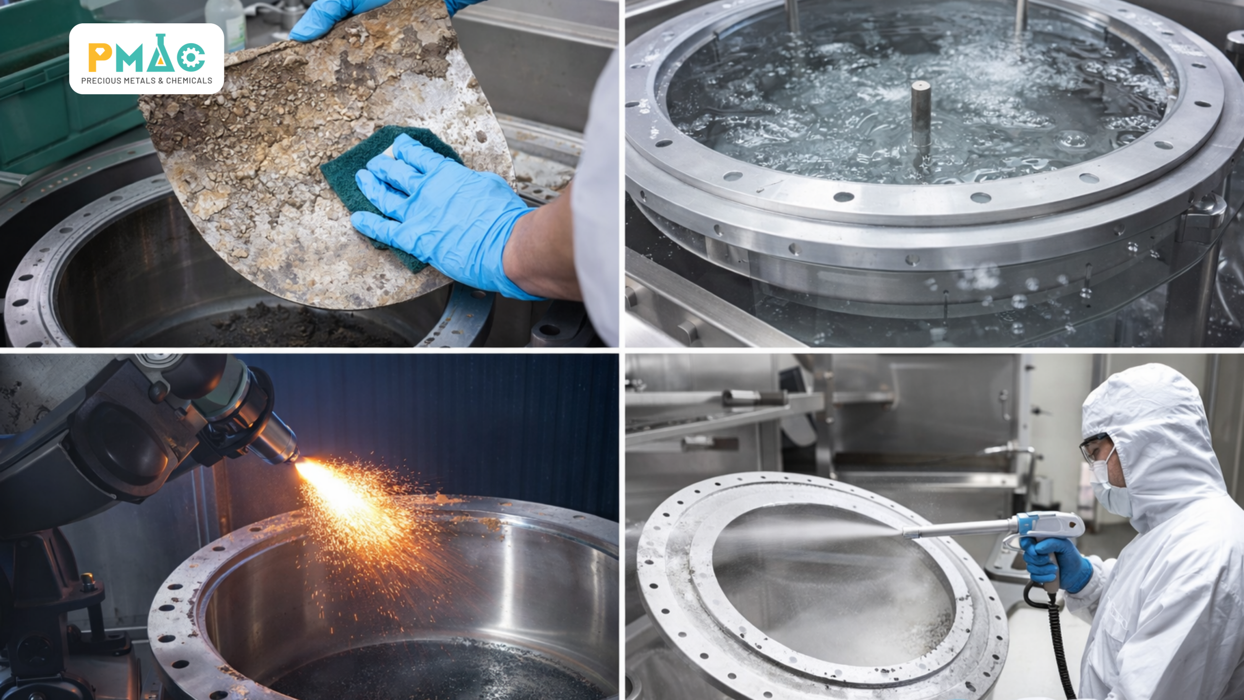
Figure 6. PVD targets require tight control of purity, composition, and surface quality
In PVD, the target is the direct source of the deposited film, so its properties have a major influence on process quality. Purity, chemical composition, density, and contamination levels can all affect the electrical, chemical, and structural properties of the deposited film.
In semiconductor manufacturing, where contamination limits are extremely strict, targets generally need to meet much tighter specifications than those used in conventional surface-coating applications. Target selection therefore needs to be considered together with PVD process conditions, equipment configuration, and the specific requirements of the deposited film.
2. CVD and ALD Precursors
For CVD and ALD, precursors serve a similar role as material sources, although the requirements are more complex because the materials must undergo transport and chemical reactions before the film is formed. Precursors need high purity, suitable volatility, sufficient storage stability, and effective reactivity under the intended process conditions.
ALD introduces additional requirements because the precursor must support self-limiting reactions and allow excess material to be efficiently removed between cycles. Precursor selection therefore needs to be considered together with processing temperature, surface material, target film properties, and deposition-system configuration.

Figure 7. Precursors are key material sources in CVD and ALD processes
3. Post-Deposition Control
After the film has been formed, analytical and metrology techniques are used to determine whether the process remains within its design limits. Data on film thickness, composition, uniformity, sheet resistance, and surface defects helps engineers evaluate film quality and adjust operating conditions when deviations occur.
A complete thin-film deposition system should therefore be viewed as an interconnected chain of input materials, equipment, process parameters, and metrology. This approach is also consistent with the broader direction PMAC is developing: connecting materials, equipment, analytical and metrology solutions, and technical support around the practical requirements of each process rather than treating individual products in isolation. More information is available in PMAC Enters a New Phase: Building an Industrial Value-Creation Ecosystem.
VIII. Conclusion
PVD, CVD, and ALD all serve the purpose of creating the material layers required for semiconductor chips, but each technology has been developed to address a different set of technical requirements. PVD has strong advantages in metallization and films deposited from solid targets; CVD enables a broad range of materials with good manufacturing throughput; and ALD addresses the increasingly demanding thickness-control and coverage requirements of advanced three-dimensional structures.
As chip architectures continue to scale and shift toward 3D designs, deposition technologies must become increasingly precise while relying more heavily on high-purity materials and advanced metrology. Within the semiconductor ecosystem, PMAC is developing an approach that connects PVD targets, CVD/ALD precursors, deposition equipment, and analytical and metrology solutions to address different process requirements throughout semiconductor manufacturing.
Opportunities for Vietnamese companies to participate in the semiconductor supply chain extend beyond the chip itself to materials, equipment, analysis, metrology, and the supporting technological capabilities behind semiconductor production.
PMAC Joint Stock Company
Ho Chi Minh City Office:
4th Floor, HUTECH Building, D1 Road, Saigon Hi-Tech Park, Tang Nhon Phu Ward, Ho Chi Minh City, Vietnam
Hanoi Office:
22B O2, Linh Dam Peninsula, Hoang Liet Ward, Hanoi, Vietnam
Hotline: +84 387 235 878
Facebook: PMAC